Analog-to-Digital Converter Design with the Photo Multiplier Tube
In the study, which combines the compressed sensing (CS) and the structured illumination microscopy (SIM) methods, an object plane should first be collected by a lens, and then the collected signal should be measured by a photomultiplier tube (PMT), located at the focal point of the lens. The recorded measurements present a measurement vector that can be utilized in the CS recovery algorithm. However, since CS recovery algorithm estimates a scene based on numerical data and the PMT output is an analog signal, the output must be converted into a digital signal. Hence, the design of an analog-to-digital converter (ADC) board is required. Here, a simple optical configuration, which converts PMT analog signal into digital signal using the ADC board, is presented.
In the figure below, experimental setup, in which the object plane is measured by the PMT and in which PMT output is converted into digital data, is showed. In this setup, a 488 nm laser source (Coherent Lübeck GmbH – Sapphire 488-20), which will be utilized in the CS-SIM experiments, is operated. Laser beam is first expanded using a laser beam expander, and then the beam is projected onto a microscope sample. The generated object plane is collected by a lens with a focal length of 100 mm. Then, the collected signal is measured with a PMT that is placed at the focal point of the lens. At this point, it is required to use an amplifier since the signal level of the PMT output is too weak. The output type of the PMT is current, so a current amplifier (Hamamatsu – H7422-50) is utilized. It should be considered that the output of the current amplifier should be voltage type since the analog input of the ADC board should be voltage type. During the experiments, it is observed that the output of the current amplifier provide negative voltage. However, since the analog signal to be driven on the ADC board must be positive, an inverting amplifier (Texas Instrument – THS4011EVM) is located between the current amplifier and the ADC board. The output of the inverting amplifier is serially connected to the oscilloscope and the analog input of the ADC board. The digital data read on the ADC board are compared with the oscilloscope results. This allows us to verify the numerical data with the corresponding analog signals. In addition, the ADC board is programmed to allow digital data to be transferred to the computer. The data transferred to the computer are also illustrated in the following figure.

Figure 1. The experimental setup for ADC Design with the PMT.
In order to operate the PMT device, the device must be supplied with voltage. It is observed that the device does not work if the PMT device is operated at an average voltage value at first. Therefore, the device should first be operated at low voltage values, and then the voltage level should be increased gradually. The optimum operating voltage range for the PMT is detected to be from 0.2 V to 0.25 V. The maximum signal level of the inverting amplifier output is measured around 2.5 V to 3 V with these configurations. On the other hand, it is seen that PMT stops when the laser intensity is increased after the PMT settings are made. Hence, PMT should first be operated at high intensity level, and then the intensity level should be reduced. In the experimental study with CS-SIM, it should be considered that the laser intensity should be maximum for the first measurement. This can prevent the PMT from stopping while data is being collected.
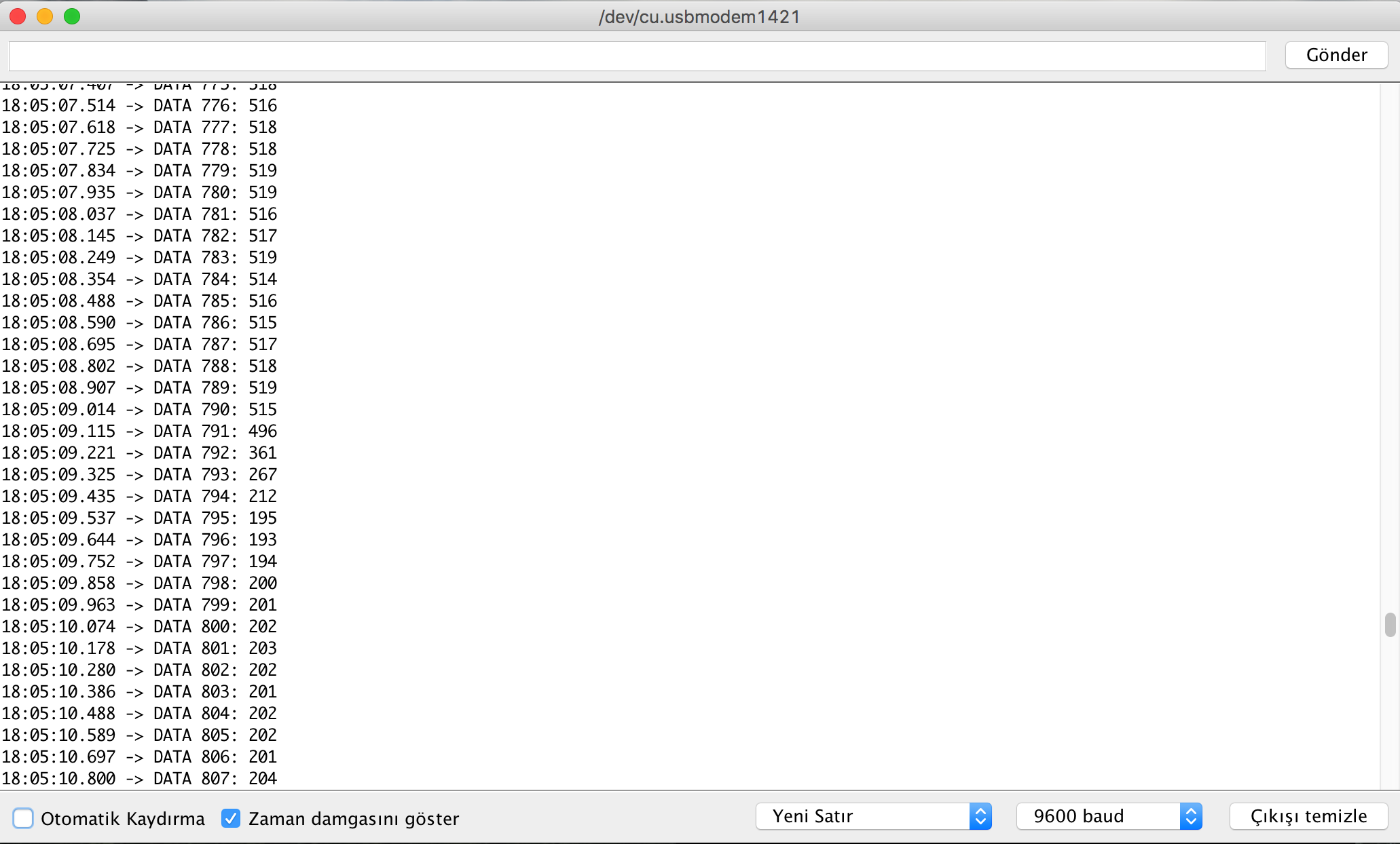
Figure 2. ADC digital data recordings.