As the title states, I partially etched some different material (Wafer 2238, 100 nm NPN) to create nanofeatures with blown out holes. With a thicker membrane, we can blow out the pores more (etch longer) without compromising the strength of the material (with regard to templating purposes). These membranes were fractured and coated with 6 nm of platinum. These images are only the NPN; not coated with gold or templated with MgF2.
Equivalent pore diameter histograms for partially etched substrates.
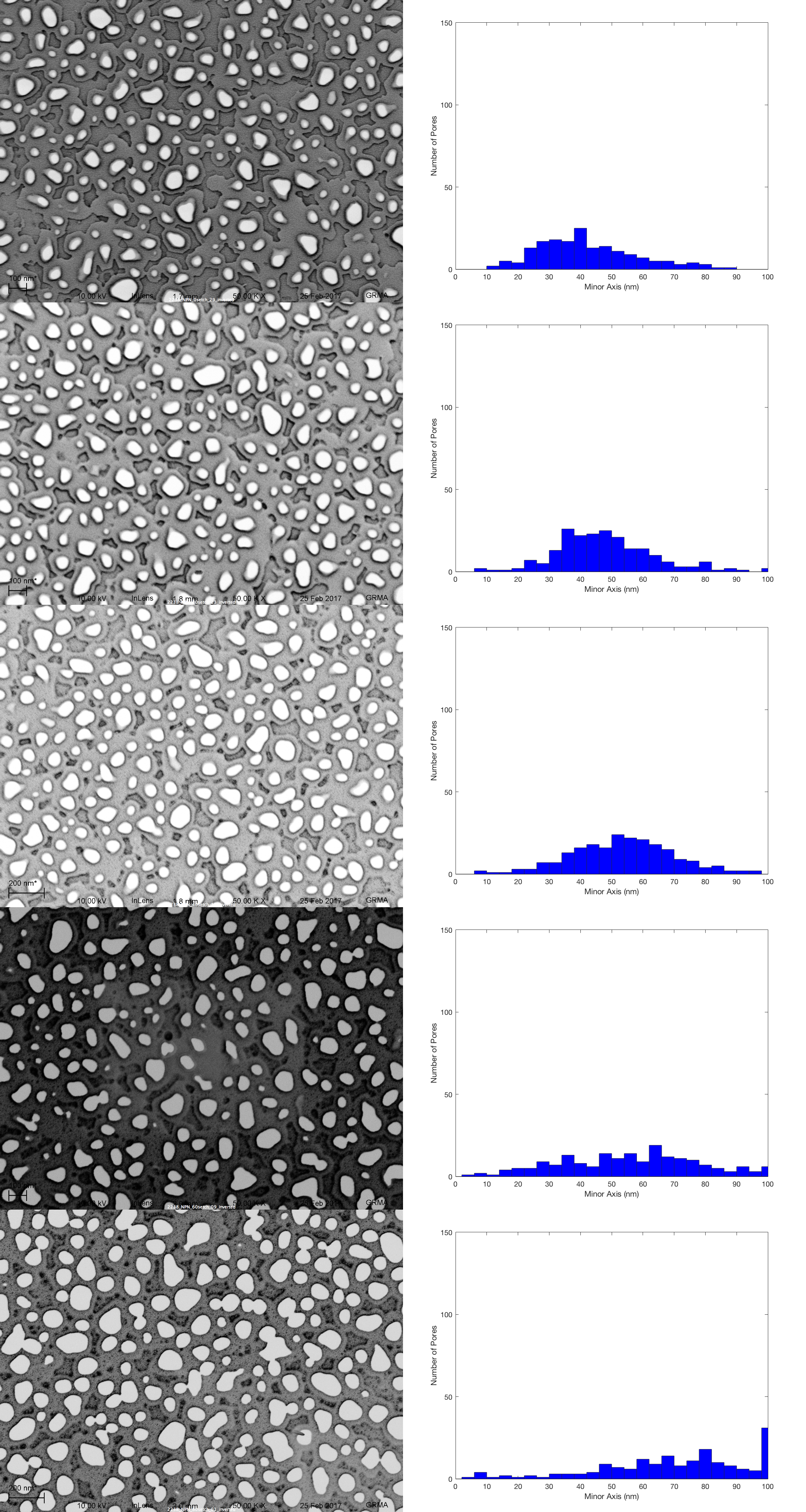
Minor Axis histograms of partial etch (0, 20, 40, 60, 80s) of Wafer 2238 (from top to bottom). Average length: 42, 48, 53, 56, 72 nm. Based on estimates of etch rate, the thicknesses of these membranes are (100, 80, 60 40, 20 nm, from top to bottom). Pores merge considerably below 40nm.
Zoom-in of wafer 2238. The scaly structures are residual pieces (siloxynitride?) used as a mask to create the thicker NPN materials. there also appears to be some conical shape to the pores, instead of anisotropic sidewalls.
Viewed off-normal, the thickness of the siloxynitride is appreciable.
40s etch crossection, 64 nm thick. (vibration hinders some resolution). The pores have a conical crossection.
80s etch aerial image. Residue pattern from the silicoxynitride is transferred through the nanomembrane’s volume.80s etch crossection. 23nm thick. The silicoxynitride acts as an etch mask (with poor selectivity) and is causing the texture at the surface.80s crossection. Shows the scalloped merged pores with sharp peaks.
I think the 2238-80s material is too weak to hold up to MgF2 processing, but there is hope for the 60s material.
Below is an image of the PDMS array on the nitrocellulose membrane. I’m trying to create a stamp that can be applied to the NC membrane, before PDMS is poured on. The idea is that the stamp will be heavy enough to keep the PDMS from soaking into the areas of the NC that the…
Hey folks, Science Saturday is this Saturday and Sunday at the Rochester Science Center. We need volunteers to man our tables from 12-4pm on both Saturday and Sunday. Please indicate in the comments of this post if you can volunteer, and when you can volunteer. The tentative schedule is as follows: 12-1 Saturday – Greg,…
Motivated by Tom’s suggestion at lab meeting on Tuesday, I tried “conditioning” the DMEM+10%FBS before adding the chips. “Conditioning” just means that I allowed the DMEM+10%FBS to equilibrate in the incubator for an hour before adding the chips to test if a brief (~1 hour) exposure to very high pH causes discoloration. DMEM+10%FBS without the…
Cindy Hartnett – professor of mechanical engineering at Louisville requested some pnc-Si chips after reading our PNAS paper. In requesting the material she mentioned … I’ve long been searching for a low-voltage way to drive some micro-actuators. Electrokinetic pumps looked good but until now the necessary voltage was far too high. About a month after…
My PhD exam was postponed (tentatively to early September but it’s up in the air still) due to an impending bureaucratic nightmare, so for the last few weeks I have been running more filter experiments, and I have discovered some interesting trends. While it is generally the case in nanopore experiments that the average dwell…
Since Jess saw discoloration last week within a day in PBS with the new material, I did a couple of discoloration studies this week. I looked at wafers 670 and 673 and compared them to 625, 704 and 680-T. These were not RTP’ed, I did the tests at RT since that’s the temp diffusion studies…