50/50 Si/MgF2 Freestanding film
Previous posts: Theory Deposition Etching Imaging First Freestanding Membranes
I had previously made free-standing nanomembranes that were mostly MgF2 according to the EDAX scan of the freestanding region:
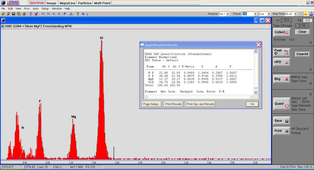
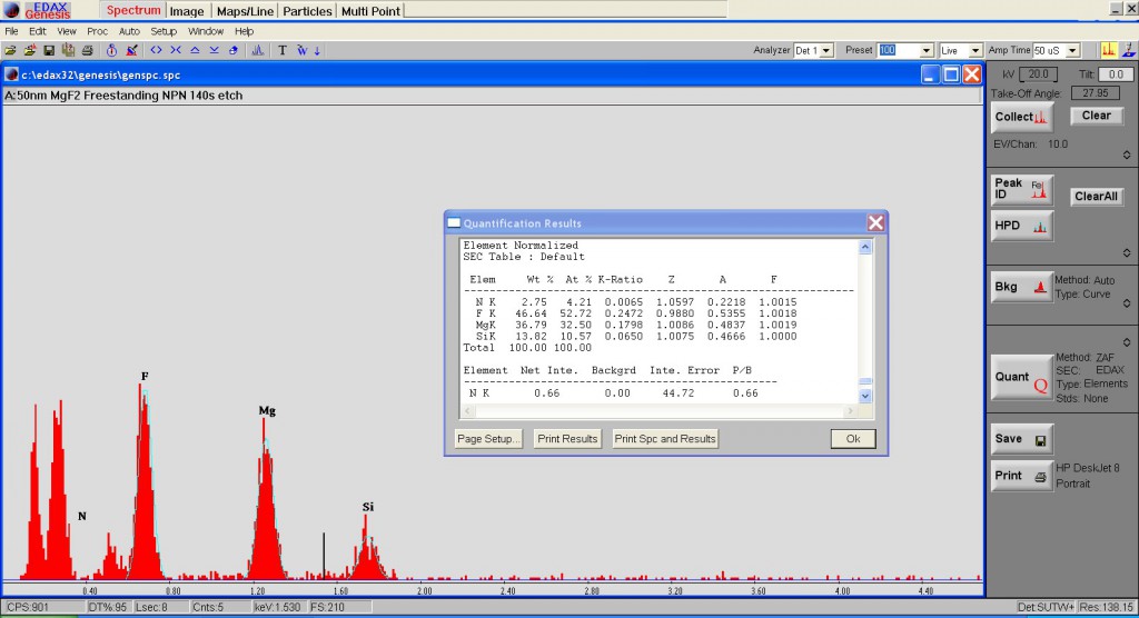
I hoped to duplicate my results and send over a few more samples to Nottingham. With that in mind, I ran an evaporation to produce a 50nm MgF2 nanomembrane (250C, 1-2 A/s, 0.5-2 mA) with a new melt (replaced old material with new MgF2 pellets). The RIE etcher had not been performing well over this period (eventually I found out the Ar regulator at the wall was nearly off) so after some troubleshooting, I recreated my etch recipe, which have slightly different flow settings on the MFC, but the same partial pressures (5 mTorr O2, 95 mTorr CHF3, 100 mTorr Ar). After etching for 150s, 180s, and 210s on separate SEPCON chips, I took a look at the EDAX signals:
By eye, the samples look the same as the previous 85% MgF2 windows. There is a teal color to the nanomembrane when viewed off angle, and the backside of the chip is mirror-like (indicating that the Si3N4 substrate is much less than 20nm thick). We probably do not see a Nitrogen peak because that characteristic X-ray is often reabsorbed, so I have been using the silicon peak as a representative for how much Silicon nitride remains on the etched film. However, it could also be that my evaporation is not as pure as it needs to be, and there may be no Silicon nitride left at all. If there was a dusting of Si on the pellets, the Si could have easily been evaporated with the MgF2, incorporating itself into the film, poorly. The tool itself is used for many different evaporations, with a number of crucibles, including SiO2 pellets. It will be interesting to see if the different film compositions produce different Raman background signatures (I believe they should).
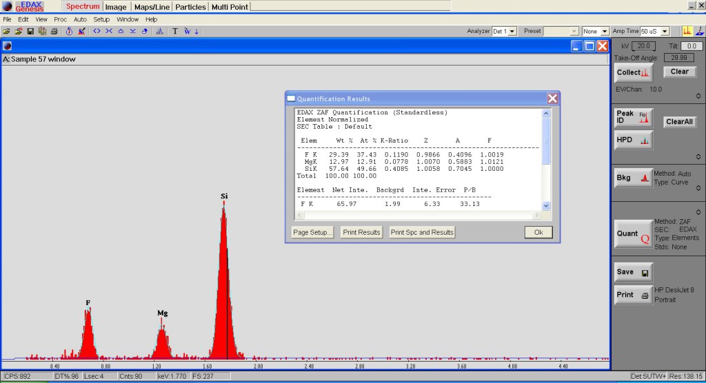
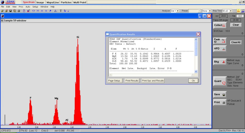
Have you looked at plain NPN samples to get a baseline? I have often found strange peaks in EDX from metals in the chamber far from the sample that is somehow getting hit with a high-energy electron and generating a X-ray. Your Si peak may not be coming from exactly where you think it is, so I would look at both an NPN membrane and a solid SiN membrane to see if you get any useful insight…
I have run a control in my previous post (unetched NPN) (https://trace-bmps.org/blog/data/2014/01/20/free-standing-mostly-mgf2-nanoporous-material), showing a carbon peak that I believe results from the tape on the holder getting hit far away from the observation space. This peak changed to Al when I switched the samples to a different holder. I should try and suspend each sample over free space and measure again (control NPN, 85% MgF2?, 50% MgF2), to see if I get the same results. When you say measure a solid SiN membrane, are you referring to a measurement in the bulk region of the NPN chips?
I see. The previous post seems to show that the N peak is visible in SiN, correct? Therefore, the scans without the N peak above, should indicate that the SiN is gone.
The “solid SiN” membrane is just a non-porous SiN membrane – SiMPore makes lots of these and there should be samples around. The issue here is that a porous membrane will allow lots of high energy electons to go rigth through the pores, which is not typical for most samples. These electrons can strike anything and generate X-rays that can easily make it back to the detector.
With this in mind, could the Si peak in the 140s etch sample, just be the background wafer signal, since the N is gone? Then as you continue to etch the porous MgF membrane, you are making it more porous and thin, allowing the Si wafer signal to increase? Just a thought….