Fabricating 0.5 um Channels in Microscope Slides for Staph Invasion Assays
Summary
After success with the development and execution of the μSiM-CA (Canalicular Array; see Masters et al., Nanomedicine: Nanotechnology, Biology, and Medicine 2019), Jim wanted to develop a platform to answer some more biophysics focused questions. In order to facilitate these studies, the platform would ideally be configured to allow for live imaging of staph invasion into sub-micron spaces. Unfortunately, the transwell setup of the μSiM-CA limits our ability to actually observe the invasion. Therefore, we decided to move forward to a device that includes long (mm) channels with 0.5 x 0.5 μm openings in glass. Over the past few weeks, Greg and I have been working in the clean room to build just this. We had some success in the process of fabrication, but the etching process needs to be optimized, as the selectivity of the resist over the microscope glass substrate is poor.
Methods
Cleaved glass microscope slides were coated with P20/HMDS and Shipley S1805 using the following spin protocol:
- 5 sec @ 1000 RPM (add adhesion reagent or photoresist in this step)
- 50 sec @ 7000 RPM
- 5 sec @ 1000 RPM
Coated slides were then transfered to 115C hotplate and soft baked for 60 sec.
The resulting slides were surprisingly uniformly coated. However, replicating this protocol on the thin and flexible coverslips may take some trail and error.
Coated slides were transferred to the laserwriter and loaded into the tool.
Using lens 5, the photoresist was brought into focus (Z ~= 1300-1350 um) for this brand of microscope slide), and the following parameters were set:
- Filter: 1%
- Pos: 2 mm/s
- Write: 2 mm/s
- Vector Mode
- Planar autofocus correction (established M1, M2, M3)
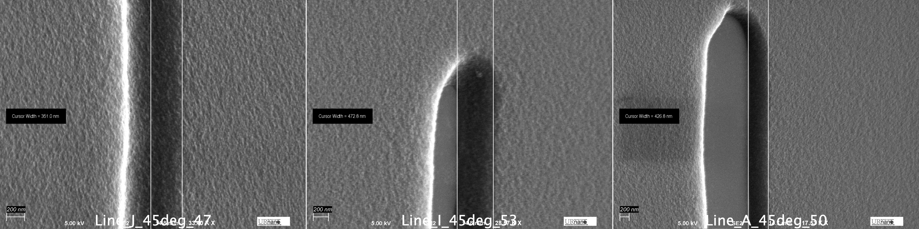
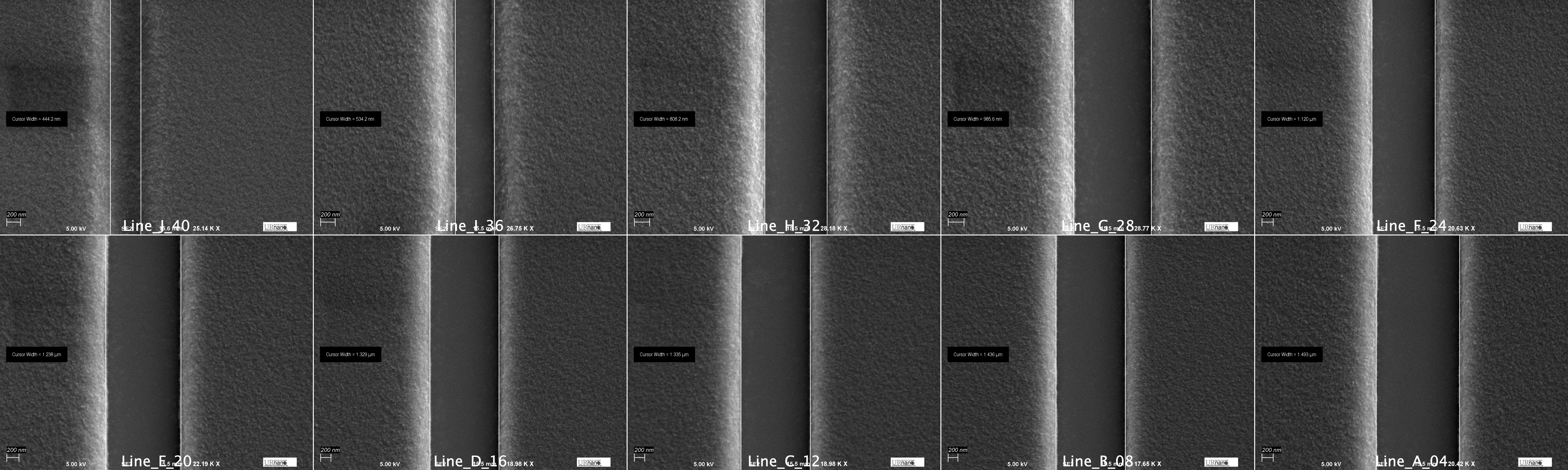
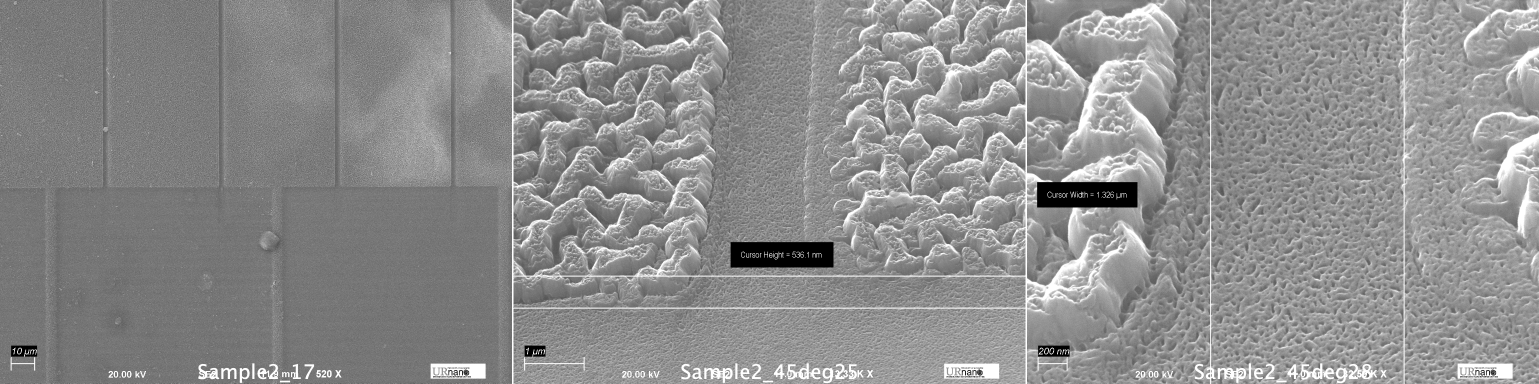
In our first run, we ran a dose-response test, starting with a gain of 0.1 and moving through to a gain of 1.2. In the ClerWin pattern generating software, we set a series of 12 doses onto different layers, allowing us to keep the same registration for the dose-array. After exposure, exposed slides were developed in MF for 30 sec and rinsed thoroughly with diH2O. Finally, slides were dried in the oven, coated with 8 nm platinum, and imaged under SEM (Figure 3).
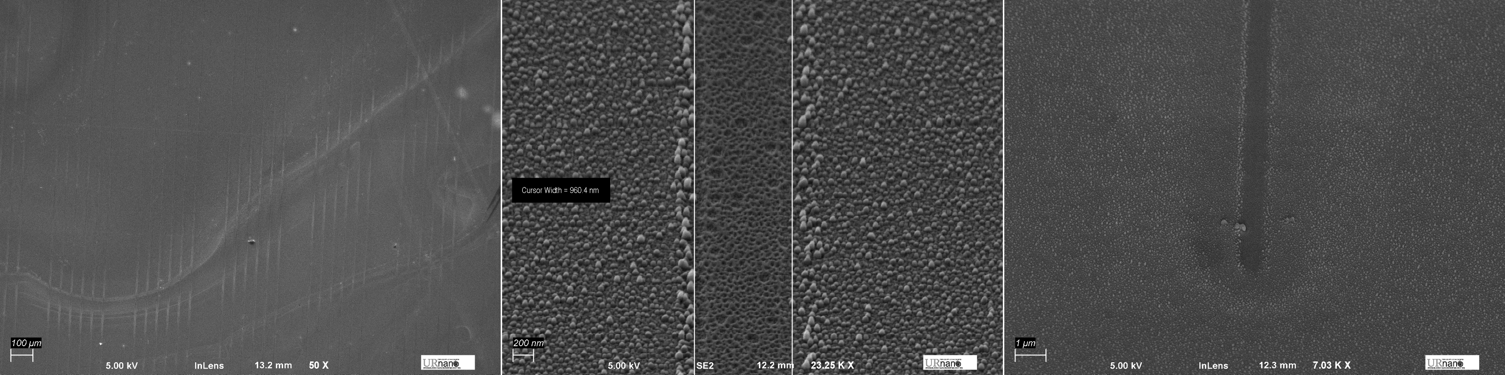
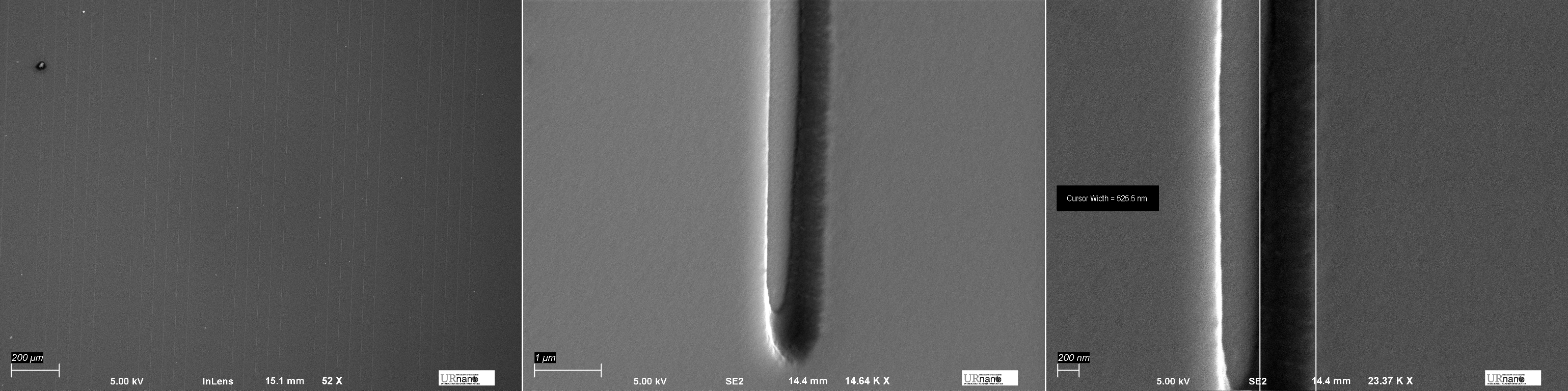
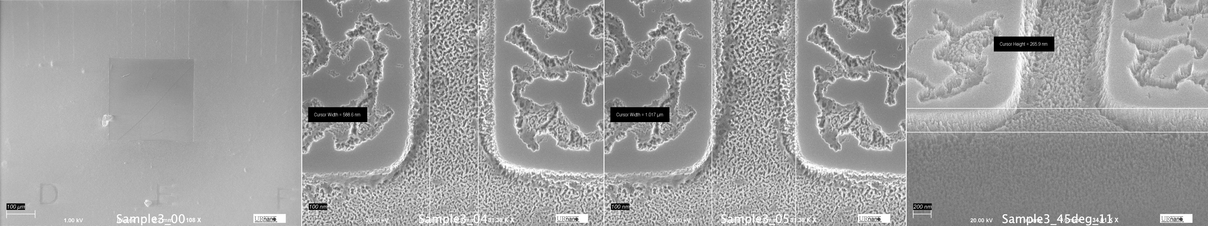
In our second run the following day, we repeated exposures for two more glass slide sections, with gains ranging from 0.3 to 0.7, again following the same development protocol. These channels were then exposed to different etching recipes (stdSF6 for 5 min and stdCHF3 for 13 min) in the Oxford RIE to transfer the pattern into the glass
stdSF6 recipe
- 15 sccm O2
- 30 sccm SF6
- 10 sccm CHF3
- 100 W
- ~100 nm/min etch rate on SiO2
- 30 – 50 mTorr etch pressure
- Known to aggressively attach photoresist
stdCHF3
- 10 sccm O2
- 45 sccm CHF3
- 100 W
- ~40 nm/min etch rate on SiO2
- 300-400 mTorr etch pressure
In our third run, we observed poor etch transfer characteristics from the previous runs so we changed the etch recipe again based on some recipes I found in literature.
Ar/SF6
- 25 sccm Ar
- 25 sccm SF6
- 175 W
- 40-50 mTorr etch pressure
- 15 minutes produced ~370 nm depth into microscope glass
- 10 minutes produced ~200 nm depth into microscope glass
Results
On our first run, 10 of the 12 doses produced noticeable features in the photoresist. Gains were A = 1.2, B = 1.1, C = 1.0, D = 0.9, E = 0.8, F = 0.7, G = 0.6, H = 0.5, I = 0.4, J = 0.3 in these montages.