Potassium Sensor Development
As previously stated in my initial post (found here https://trace-bmps.org/nanomembranes-in-potassium-ion-selective-electrodes), I am in the process of developing a potassium Ion Selective Electrode (ISE) Sensor using our chips. Along the way I have gathered all sorts of curious but interesting data, with observations bringing both old discoveries and new oddities to light. Outlined below are some of these findings as well a narrative of how we think they have come about and why we think they may be good or bad.
*See The Highlight Reel at the end of this post if you are only interested in a quick summary
The Beginning: Literature Based Experimentation and Familiarization with Gel and Chip Interaction
After a thorough literature review, I decided to begin attempting to develop a polymer ISE resin. Based upon well researched values, the first polymer matrix I made consisted of 33 wt% Polyvinyl Chloride (PVC), 66 wt% Dioctyl Sebacate (DOS), 1 wt% Valinomycin (Val), and 50 mol% (based off of Valinomycin) Potassium Tetraphenyl Borate (KBPh4). This mixture is fluid enough to allow valinomycin to travel between surfaces freely but is solid enough to retain its components over long periods of time. For use on a few chips at a time these components are dissolved in 2 mL of Tetrahydrofuran (THF) which acts as the solvent for this entire system. Once in this gel form the PVC layer is ready to be deposited onto the chips.
Dip Coating and Drop Casting
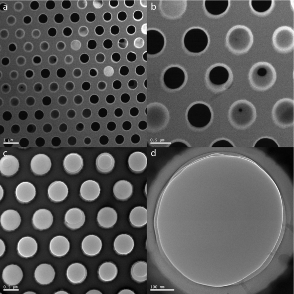
Initially I tried two different methods to coat the chips in this potassium selective layer: dip coating and drop casting. Both of these methods were tested on 0.5 micron chips with variations of dipping times and drop casting methods. The results were similar across the board, with seemingly uniform coverage of the windows for both methods. The biggest difference between the two arose from the thickness of the gel layers on the chips; dip coated chips had thick layers of gel while drop casted chips had thinner layers of gel. Upon analysis with SEM it was found that for both methods the gel layers were too thick to gather any meaningful data. This is shown in Figure 1 below where the bottom darker area of the image is the drop cast gel and the upper spotted area is the exposed microporous membrane.

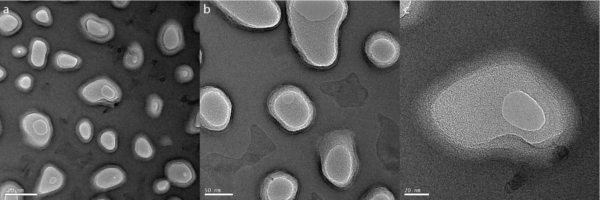
In lieu of SEM analysis, we attempted to analyze the gels with TEM to provide more information on whether or not the gels were filling the pores of the membrane. To aid in this pursuit we ditched dip coating and used small volume drop casting to limit gel thickness on the membranes. This proved more fruitful for analysis and TEM images were able to be captured showing that while some pores were completely filled with gel, pore fill was not uniform across the entire membrane. This is shown in Figure 2 below. Interestingly you can see in Figure 2d that the filled pores have a meniscus form. This suggests that the gel within the pores may be even thinner than the membranes themselves. Nonetheless the problem of complete pore fill remained.

Sepcon Funnel Centrifugation
In an attempt to fix this problem we tried a new deposition method using sepcon funnel centrifugation. We did this by loading chips into sepcon funnels and depositing gel on top of the chips. We would then centrifuge the funnels which would force the gel through the pores of the membrane. This process is shown in Figure 3.

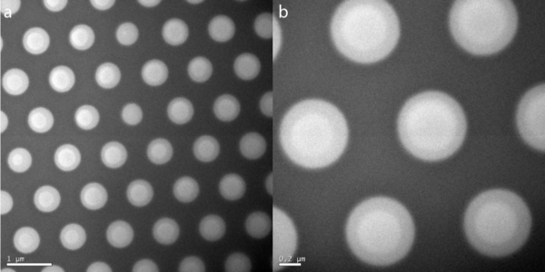
We first tested this method on 0.5 micron chips and found that it worked better than both dip coating and drop coating. This method excelled at filling every pore with gel, but the issue remained that not all pores were completely filled. TEM images of these chips showed that while most pores were filled completely with gel, some only had a small ring of gel around the inside of the pore. In addition there were also some pores which were mostly filled but had small pockets which were left unfilled. Results are shown in Figures 4.
To see if pore size affected the ability of the gel to completely and uniformly fill a membranes pores, we used the same sepcon centrifugation method with nanoporous membranes. As shown in Figure 5 this did not solve our problem and it seems like pore fill was more or less the same as with the 0.5 micron chips.
Evaporative Deposition
Still lacking complete pore fill we attempted to fix this problem by trying a new technique: evaporative deposition via sepcon funnel setup. This was done by loading chips into sepcon funnels and adding gel to the top sides of them. The sepcon funnels are then sealed so that airflow can only proceed through the pores of the membrane. The result of this makes it so that the evaporation of the solvent (THF) has to go through the pores, in doing so the gel is pulled tight into the pores of the chip. This process is illustrated in the diagram shown in Figure 6.

In conjunction with testing this new method of deposition, we also made gels with varying ratios of plastic to plasticizer in order to change the viscosity of the gel layer. In doing so we wanted to determine if the viscosity of the gel had any affect on the ability of the gel to completely and uniformly fill the pores of a membrane. The results of these experiments showed that evaporative deposition as a whole worked better than the other methods used before. The experiments also showed that viscosity does indeed affect the ability of the gel to fill the pores. Testing ratios ranging from 20:80 to 60:40 weight percent plastic to plasticizer, we found that the 20:80 ratios was the best for filling 0.5 micron pores. The results from these experiments are shown below in Figure 7.
As shown in these figures complete pore fill was accomplished with the 20:80 polymer gel. Interestingly enough we were also able to determine that gel viscosity effects the ability of gel to completely and uniformly fill pores across and entire membrane. This was determined after most of the other gel ratios produced chips which were clearly not filled with gel. Ultimately we were able to conclude that evaporative deposition is the best method to use to achieve complete and uniform pore fill across and entire 0.5 micron membrane using 20:80 gel.
Reproducibility and Layer Optimization
Successful pore fill allowed for our focus to be changed to reproducibility and to adding the remaining layers necessary to make the electrode functional. At the same time access to the TEM became very limited. To prevent this from slowing our progress on the project we began to analyze layer deposition using light microscopy.
Gel Deposition Reproducibility and Gel Ratio Optimization
To determine the reproducibility of the results shown above we used the 20:80 gel and deposited it onto triplicate sets of 0.5 micron chips. In addition we also deposited this same gel onto 3 micron and NPN chips to determine if this gel ratio would work with different sized pore systems. Results showed that the 20:80 gel did not fill the 0.5 micron windows as well as they had before. While there were areas that were as filled as before, there were also large spots of unfilled pores. Areas that were filled look uniform, but the unfilled areas showed us that the results were not reproducible. We determined this was most likely due to the fact that we were close to the optimal viscosity for the 0.5 micron windows, but not quite there.
Surprisingly the 20:80 gel did not do a sufficient job at filling the pores of the 3 micron chips or the NPN chips as well. With the 3 micron chips very little pore fill took place. With the NPN chips the gel layer was too thick and the windows pulled out of them. From these results we determined that not only does viscosity of the gel matter when filling the pores of a chip, but the size of the pores changes the viscosity requirements for the gel to completely and uniformly fill a chips pores.
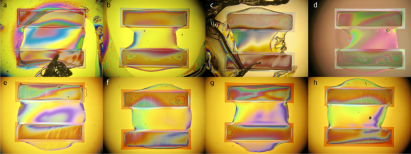
To determine what the optimal ratio of plastic to polymer is for 0.5 micron chips, we tested 15:85 and 25:75 gel. Concurrently we began taking light microscopy images to analyze our pore fill. As shown in Figure 8, both gels had good pore fill but pulled away from the corners of the windows. When comparing the uniformity of both of the layers it was determined that the 25:75 ratio was better than the 15:85. Because of this we proceeded forward using the 25:75 ratio. Nonetheless it was interesting to see in Figure 8b creeping of the gel when entrapping the hair like contaminant on the surface of the chip. This suggests that the gel has a strong affinity for binding to itself and potentially to similarly charged particles.

When imaging these chips I accidentally knocked a window out of one of them. Upon imaging this window it can be seen that the gel permeates the structure so well that it holds the shattered pieces of the window together. This is unique to pore fill with gel and also indicates complete and widespread pore fill. The image of this is shown below in Figure 9.

Testing the Limits of the Optimized Gel
In determining the reproducibility of the 25:75 ratio gel, we evaporatively deposited gel onto more 0.5 microporous chips. In addition we also evaporatively deposited this same ratio gel onto 0.5 micron slit chips to see if there would be a difference in deposition between slits and pores. As shown in Figure 10, similar successful results were reproduced. This suggests that the 25:75 ratio is correct for 0.5 microporous chips.
With this round of chips de-lamination of the gel was observed for the first time between the gel layer deposited within the pores of the chips and the excess gel left behind in the sepcon funnel. This can be seen in Figure 10 as curved lines spanning the height of the windows. This reinforces the idea that the gel adheres to itself strongly and is not easily taken apart.
When deposited onto 0.5 micron slit chips similar behavior of the gel was observed as with previous gels deposited onto different size or shape pores. As shown in Figure 11 gel was able to fill a majority of the membranes but it notably oozed through and came in contact between each window. This again shows the desire for the gel to adhere to itself, but it also shows that this ratio of gel is too liquid for the larger slits and that the size difference between pores and slits provides a notable performance difference from the gel.

The continued challenge to completely fill the windows in the corners left uncertainty to whether or not the edges were actually porous. To test this theory we evaporatively deposited 25:75 gel onto 0.5 micron non-edge aligned chips which are completely porous throughout the entirety of the window. As shown in Figure 12 below this seemed to fix our problem with filling pores up to the edges of the windows, but the delicate nature of these windows caused many of them to break. Nonetheless it was shown that again the gel holds together the broken windows and that this ratio works fairly well for this pore size. This conclusion therefore suggests that unfilled corners in the regular 0.5 micron chips are actually nonporous and the windows are completely filled.
To determine how quickly these gels set within our membranes, we conducted an experiment using 0.5 microporous chips and 25:75 gel imaging chips at set time points. Under the same conditions we pulled chips out of their sepcon funnels after 5 minutes, 30 minutes, 60 minutes, 120 minutes, 180 minutes, 240 minutes, 300 minutes, and overnight. From this experiment we saw that any gel under 180 minutes was much too liquid to be set within the pores. After 180 minutes all of the gels were solidly set in place, determining this as the minimum amount of drying time for the gels. Also apparent in all of these chips was the tendency of the gel to ooze through the membrane to come in contact with the gel coming through the other window. These results are shown below in Figure 13.
Also with this set of experiments we tested the affects of vacuuming a gel through the windows using the sepcon funnel setup. As shown in Figure 14 the gel was pulled through to form an interesting dimpled surface on the chip. We hypothesized that this occurred after the gel was quickly pulled through the pores and simultaneously dried.

Thin Film Experimentation
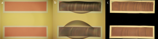
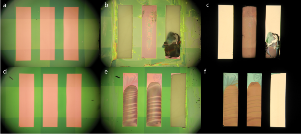
With the PVC layer beginning to be successfully reproduced, we began to try to develop our electrode layers as thin films to ascertain that they work well before trying to miniaturize them onto a chip. We began by trying to drop coat our 25:75 gel onto a cleaned piece of 0.01 inch thick copper foil. This ended up drying without expanding very much creating a hundreds micron thick layer of gel. Wanting a thinner layer of gel we attempted to spin coat using a small spin coater in our lab. Initially the spin coater was too slow and the gel was not spread evenly in all directions. Speeding up the spinner led to a more even and thinner coat. Satisfied with this layer, we then tried to spin coat our solid contact, PEDOT:PSS, on top of a piece of copper foil. This spun out easier than the gel and could be done at a lower speed. Both results can be seen in Figure 15.

With the ability to spin coat both of these layers independently, we went ahead and tried to spin coat the two layers on top of one another. In doing so we found that thin layers of these two materials do not bind well with their polarity differences causing the layers to pull away from each other. This required that large volumes of both layers were needed in order to deposit layers that would stay together without pulling apart.
Building the Chip Electrode: Layer Deposition
Our first attempt at depositing these layers onto our chips was via drop casting. Seeing as our focus was making the electrode work we momentarily put our pore filling procedure to the side and focused more on testing the ability of the layers to work properly. Initially we drop cast 50 microliters of 25:75 PVC gel into the trench of NPN chips. This filled the trench and spilled over slightly onto the flat surface of the chip. Once this layer dried we would then drop cast 3 wt% PEDOT:PSS on top of it. While this layer would deposit across the membrane uniformly, drying would make the material pull away from the PVC layer and pull apart. No matter how many times PEDOT:PSS was deposited afterwards the layer would continually pull away from the PVC layer. In an attempt to promote adhesion of the two layers we tried to vacuum the drop cast PVC gels to make them dry quickly and hopefully dimple as we had seen in our earlier experiments. This did not create many surface artifacts proving that the dimpling seen before was produced as the gel was pulled through the pores of the membrane. In another attempt to promote adhesion between the two layers we attempted to dissolve the PEDOT:PSS in a more polar solvent, ideally one with a polarity closer to that of THF which is the solvent for PVC. Unfortunately we were not able to get PEDOT:PSS to dissolve in any other organic solvents (ethanol, DMSO, or acetone) and we were forced to continue using water. Eventually we began trying to deposit larger volumes of PEDOT:PSS onto the chips in order to cover the entire chip surfaces. This allowed the layer to dry without pulling away from the PVC layer and without pulling apart from itself. This finally solved our problem of layer deposition and allowed us to start testing the functionality of the layers. Figure 16 shows the layer deposition process on the chips.

When making these chips we noticed that when the they were laid on a flat surface and the PVC layer was deposited onto them, some PVC would permeate through the membrane and dry on the opposite side of the membrane. We hypothesized that this must occur as the solvent for PVC (THF) evaporates. When laying against a flat surface the THF will evaporate through and then collect on the flat surface, potentially condensing and wetting the other side of the chip. This provides a bridge between the two surfaces allowing the PVC to permeate through the pores. To test this idea we deposited similar PVC gel onto NPN chips which we setup to be floating having no surface contact on either side of the membrane. After drying it was found that no PVC had permeated across the membrane thus confirming the ideas aforementioned. Images of the opposite side of these chips were taken, one of which is shown in Figure 17.
Prototypes and Ion Selective Electrode (ISE) Functionalization
With the ability to reproducibly create these layered electrodes on the small scale of our chip we turned our attention to testing if the systems that we made actually worked and how well they worked. Our ideal ISE would selectively bind to potassium and only produce a change in electric potential from potassium ions. It would be able to work with potassium concentrations in the range of 1 mM to 10 mM which is the range of physiological blood potassium concentrations. On top of this it would be able to work off of a small volume of sample and be able to separate potassium ions out of the complexity of blood. An ISE that could complete all of these functions reproducibly and accurately is what we strive to create. While testing the ISEs themselves we also began building prototypes of the handheld system as a whole to try to incorporate some design ideas into our work. This included building various test circuits, test strips, and a handheld testing device. To encapsulate what we were envisioning we developed the animation shown in the animation below. This shows what the entire system would look like and how we think it would work.
Designing and Developing Test Strips
To design our system to be familiar with as many people as possible, we attempted to mimic the design of the already commonplace glucometer system. This system utilizes small disposable test strips which act as a transport vehicle for glucose in the blood to get to the sensor within a handheld digital device. These strips are often made of plastic or paper and utilize capillary action to draw a small volume of blood up the strip into the glucometer device. Our strip design is loosely based off of these glucometer strips shown in Figure 18 below. These strips are made up of multilayers of plastic which hold copper electrodes and gelled chips within them. On one end our chips are exposed for sample application. On the other end copper electrodes are exposed which are connected to our selective and reference electrodes (either separate chips or separate windows of one chip). This design allows for a small volume sample to be applied to one end of the strip and inserted into the handheld device to be analyzed.

The interior circuitry of this handheld device is relatively simple, carrying out simple interface functions and processing electrode potential produced by the selective electrode strip. Shown in Figure 19 below we began by making a simple interface circuit on a breadboard. This contained a power source, power switch, microcontroller, buttons to control the interface, temperature sensor, low pass filter, differential amplifier, and a LCD display. With these components the device could process the signal received from the electrode, take into account the temperature at the time of testing, filter noise out of the signal, and amplify this signal to be processed through the microcontroller and ultimately displayed on the LCD as a concentration. Further iterations contain the same components just in a more compact setup.

While these prototype breadboards and hand held device were functional, most of our testing was done with a simplified version of these circuits. This was a result of our focus being on testing the ISE and making sure it worked properly before we refined our hand held device. The design of this circuit is shown in Figure 20.

Testing ISE Function
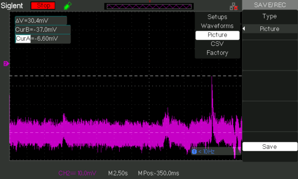
We began testing by using the thin film copper foil electrodes to see if the layers would work properly before we tried testing them on a chip. We did this by first seeing if these layers would produce a selective signal with different concentrations of KCl and NaCl. This was done by dipping the spin coated copper pieces into different concentration solutions of each and recording their response after equilibration. As shown in Figure 21 below these electrodes showed selectivity for potassium ions over sodium ions. They also showed a concentration dependent signal proportional with a decrease in concentration.

Unfortunately each test required a minimum of 5 minutes to achieve a properly equilibrated signal, therefore developing the need for a quicker response time.
With the thin layers successfully tested we deposited these layers (via drop casting) onto test strips instead of spin coating onto copper sheets in order to miniaturize the setup. Testing with these test strips showed the same selectivity for potassium over sodium as before, but as shown in Figure 22 we no longer saw the relationship between ion concentration and mV response that we saw before.

The loss of our concentration relationship was attributed to layer de-lamination which was observed during experimentation. To combat this we attempted to spin coat the layers into our test strips. Testing showed that this reinstated the relationship that we saw earlier but at a desired shorter timescale. As shown in Figure 23 responses that we got from this system provided a peak which gradually decayed over time. This told us that the ISE was working properly but that the electrode’s stability was not good over small periods of time.

Despite this we continued testing these thin film test strips to determine their response to different concentrations of KCl. As shown in Figure 24 we regained the relationship of electrode response and potassium concentration where an increase in one led to an increase in the other. In addition we found a decrease in signal response after we tested if test strips could be used more than once. We therefore determined that these electrodes cannot accurately be used more than once.

Concurrently we also found that these electrodes still exhibited selectivity for potassium over sodium as shown in Figure 25. While the selectivity found was only two times greater for potassium over sodium, further optimization of the layers should allow for an increase in potassium selectivity.

Wishing to solve some of the stability problems shown with these experiments we switched back our focus to layering these materials on our chip in a manner that would ameliorate these issues.
Testing the Chip Electrode
With the layers deposited onto 0.5 micron chips, we attempted to complete the same tests as above. We quickly found out that allowing the layers to dry on the chip and then applying the chip to the copper electrode created an insufficient surface contact between the two. This prevented the electric potential produced by the ISEs from being transferred from the chip ISE to the copper electrode. To fix this we began using the solid contact layer as a glue to the copper electrode in conjunction with its transducing role. This fixed our surface contact issue and allowed us to collect measurements from these electrodes. Despite the same layer construction as before, results gathered with these chip electrodes were vastly different than what we captured before. As shown in Figure 26 our ISE response was no longer sustained. Instead we observed a signal that was instantaneous with contact of analyte to the ISE which diminished almost immediately.
No matter the concentration of of KCl we tested, the duration was the same while the magnitude of the peak changed instead. Testing different concentration of KCl we found that we have again lost the direct relationship between concentration and electrode response that we had seen before. Instead we now find and inverse relationship between the two variables. In addition we have also lost our selectivity for potassium over sodium. This data is shown below in Figure 27 and Table 1.
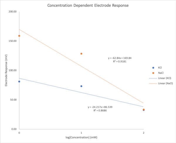
| Average Responses | |||
| KCl | NaCl | ||
| Concentration (mM) | log(Concentration) (mM) | Response (mV) | Response (mV) |
| 1 | 0 | 81.10 | 159 |
| 10 | 1 | 73.20 | 128.67 |
| 100 | 2 | 32.67 | 33.32 |
Table 1: Average electrode response as ion concentration increases with repeated testing on the same electrodes
With these unexpected results we continue to move forward to try to make a reproducible and accurate device. Seeing different responses for different concentrations and different ions is encouraging but the unpredictable responses show that further optimization is necessary. We hypothesize that the odd chip electrode responses have to do with our testing circuit rather than our chip electrodes themselves. Because the testing circuit amplifies the difference between our reference and selective electrode, one hypothesis is that our layers are allowing nonspecific ions to diffuse across creating signal in both electrodes. With higher concentrations more unspecific diffusion occurs increasing the response from both electrodes therefore decreasing the difference between each electrodes response. This would explain why at higher ion concentrations the signal is lower than at lower ion concentrations. Another hypothesis is that the ISEs are being tested at the top of their ion limit and are therefore saturating. Both hypothesis present valid ideas which need to be tested in the future.
Moving Forward: Optimizing the ISEs
With all of the results collected thus far we have seen scattered success which has been challenging to reproduce. Moving forward we plan to test the two hypothesis mentioned earlier. To test the first we plan to try to thicken the PVC to make it harder for nonspecific ions to diffuse freely across the membrane. We also plan on trying to increase the plastic ratio in the PVC to try to harden the gel layer with the same goal. Overall we will try to change variables to attempt to make the gel layer harder to bypass without specific valinomycin shuttles. To test the second hypothesis we are going to complete the same experiments as above but at a millimolar concentration span. This will allow us to see if we are indeed saturating the sensors and if we just need to adjust the range at which the ISE work at. Once we are able to effectively control and understand the results of these chip ISEs we will then be able to focus on refining the testing circuitry and handheld device setup. In addition we will also try to reincorporate our chip ISEs back into our test strip design in order to prepare the system for actual testing. Once proven to work well with standard solutions we will also begin testing with blood to see if our sensor will still work with a more complex solution. Overall we have shown that this technology has potential, but there is still a lot of work to be done.
*The Highlight Reel
- We are able to completely and uniformly fill our membranes with polar gels using evaporative deposition while taking into account pore size, shape, and gel viscosity
- Gels can be manipulated through, on, and around our chip membranes with thorough control
- Thin layer ISEs can be developed but have proven to be challenging to control therefore producing results which are neither reproducible or sustainable
- Development of a handheld testing system is achievable with simple prototypes already made
- Ion testing results have been mixed, success in terms of predictable results have been scattered but evidence of an unoptimized but functional system are present
In short, we are off to a good start but there is still a lot of work to do