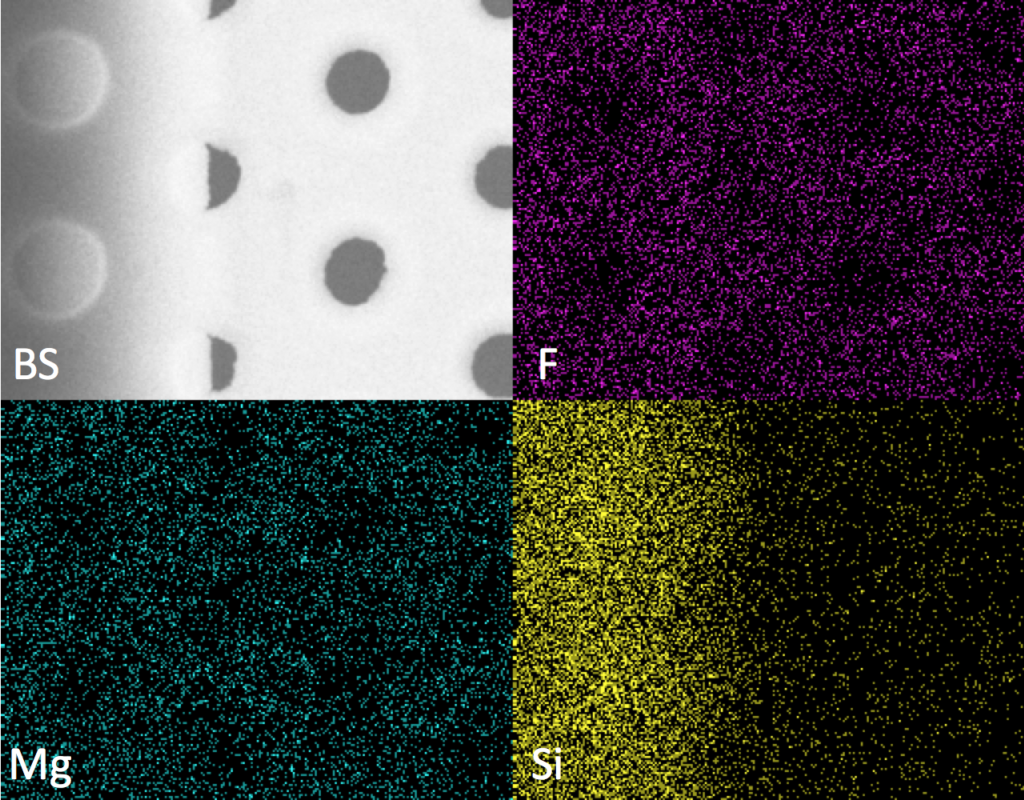
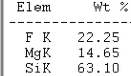
Microporous (0.4 um) MgF2 has roughly the same material purity as nanoporous MgF2

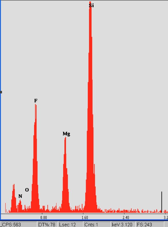
I was concerned that even though my calculations for etching the microporous MgF2 material show that the silicon nitride was being removed completely, not all of the silicon nitride was indeed being removed. Hypothetically, the presence of additional remnants of silicon nitride could be causing additional film stress and cause membranes to break more frequently. I took a few EDS measurements to confirm the material purity.


montage
EDS signals from Freestanding MgF2. The pattern of holes is apparent in the Mg and F signals, but not so obvious for the silicon. There was some sample drift, so I will have to redo this measurement, which can take an hour or two. Ideally, we can get a sense of the noise of the measurement by looking at the void space in the freestanding region.


Background:

Background of microporous MgF2. Large amount of silicon present in signal, taken in the bulk region.

screen-shot-2016-10-17-at-2-30-10-pm


Freestanding:

Spectrum after etch, in the freestanding region.  The amount of silicon is reduced. Other signals, such as Al are generated from the EDS beam passing through and striking the holder underneath.
Spectrum after etch, in the freestanding region. The amount of silicon is reduced. Other signals, such as Al are generated from the EDS beam passing through and striking the holder underneath.

screen-shot-2016-10-17-at-2-30-55-pm


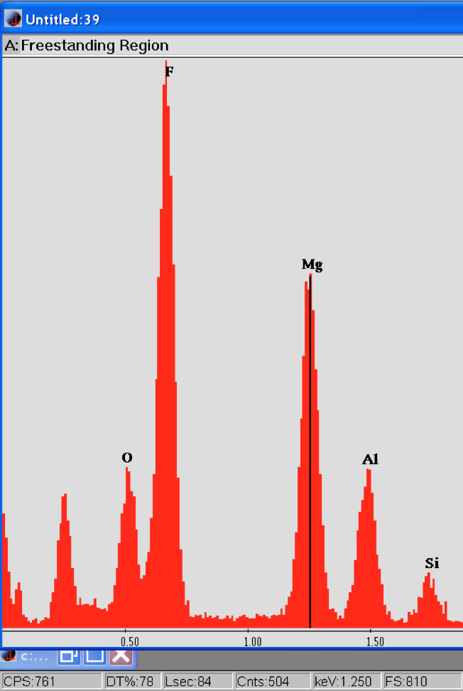
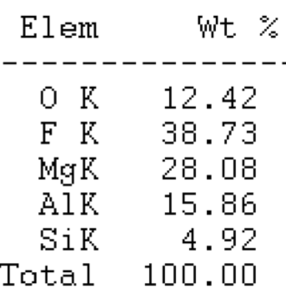
This is about the same level of material purity that my nanoporous MgF2 exhibits (85% MgF2).

Similar Posts

Leave a Reply