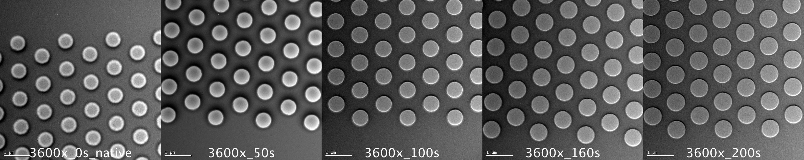
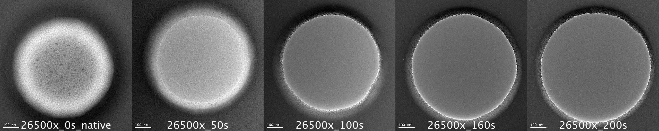
Backside Etches of 4682 Release and Widen Pores
We have a wafer that did not clear 500 nm pores (400 nm thick silicon nitride, #4682). There are about 230 chips that could be useful if they were etched a little.
I used a SF6 based recipe (15 sccms O2, 30 sccms SF6, 10 sccms CHF3, 110/10 W FWD/REF power, 5e-5 torr base pressure, 30-50 mTorr etch pressure) for varying amounts of time (0, 50, 100, 160, 200 seconds) to see if we can get porous material. The quoted etch rate is approximately 40 nm/min for silicon. The chamber was cleaned with an oxygen plasma, then seasoned with the etch recipe for 5 minutes. We etched the membranes from the trench side by placing the membranes facedown on a carrier wafer inside the etch chamber.