Thin (5 nm) Au layer TEM imaging on 1148 NPN/npMgF2
Intro
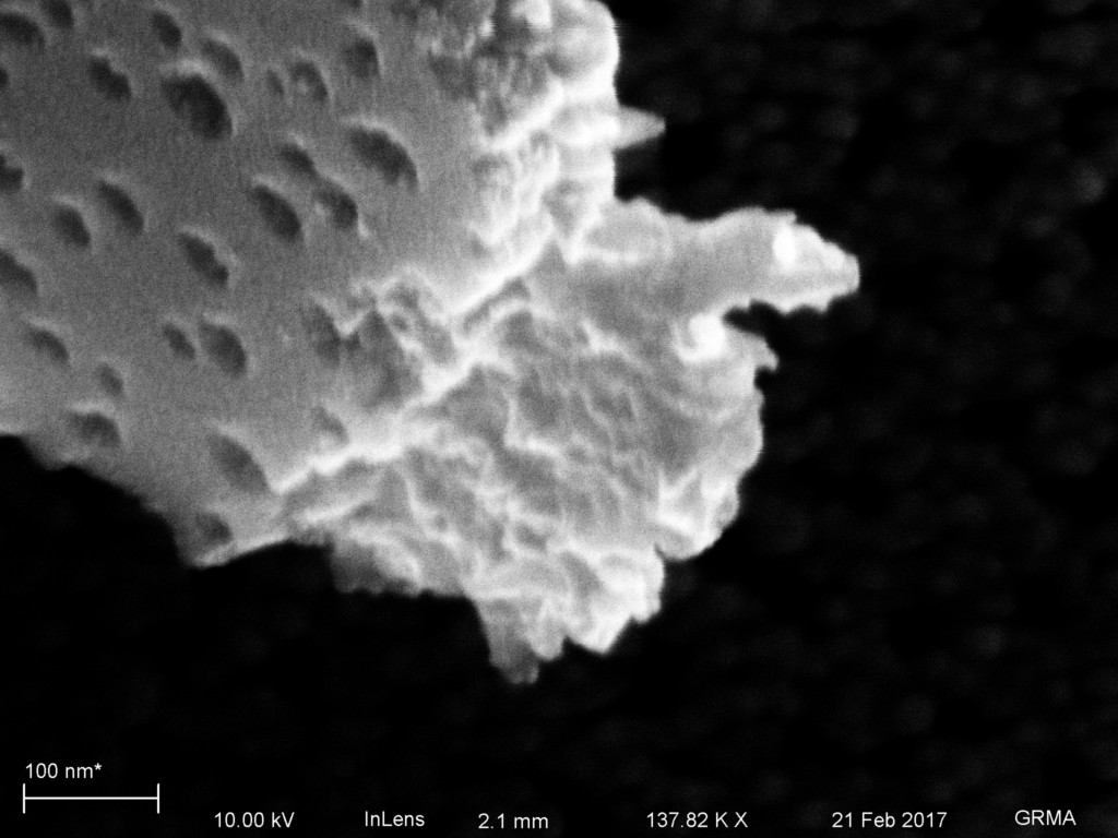
Understanding how the Au film coats the inner part of the npMgF2 is essential to understanding how the photonic properties of the npAu/npMgF2 sensor arise. From SEM, we are able to resolve little cones of Au, but unable to see how rough/homogeneous/open the Au layer is. Our hypothesis is that these little cones of Au provide large amounts of SERS enhancement because it can maximally illuminate molecules that pass through the nanopores; we surround the molecule with electric field enhancement from plasmons in the Au layer.
The images below show wafer 1236 in SEM mode, showing the different layers of the process, but not to the level of detail that we would like.

Procedure
- Evaporated MgF2 onto 1148 NPN using Kurt-Lesker PVD
- 6KVoxide, platen rotation
- Did separate runs of 150C, 250C, and 350C to observe differences in grain size
- Deposition rates were between 0.5 and 2

- Sputtered Au onto film stack using Denton Sputterer
- 15 mA current, 50 seconds (approximately 0.1
 , targeting 5 nm.
 - No platen rotation available. If we switch to the Kurt-Lesker PVD, we can have the platen rotation
- All films were sputtered at the same time; they have the same Au coating.
- 15 mA current, 50 seconds (approximately 0.1
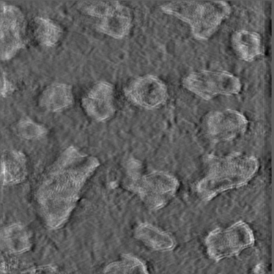
- Gathered Tilt stacks using FEI TEM
- 200KV images, gathered from at least -14 to +14 deg.
- depending on alignment, stage behavior, I can get more/less range
- 200KV images, gathered from at least -14 to +14 deg.
- Processed Tomograms
- Ran Linear SIFT alignment on images
- Background subtraction and tomogram processing with TomoJ
- Weighted Back Projection (WBP), 500 pixel stacks, which were cropped to reveal relevant features.

150 C NPN+MgF2+ 5 nm Au
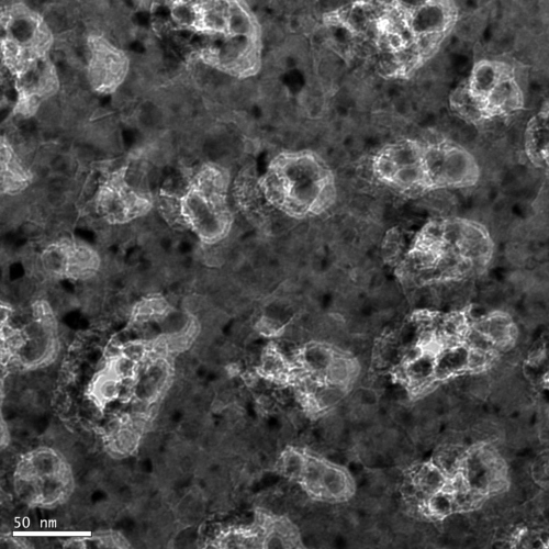
250C NPN+MgF2+5 nm Au


350 C NPN+MgF2+ 5 nm Au


Observations
- We cannot see any NPN features; it’s very homogeneous and acts like a grey level mask.
- In the future, I will etch away the NPN to reveal more detail
- Au nanoparticle sizes were somewhat inconsistent from sputtered films, ranging from 5-20 nm.
- This may be adjustable with different sputter settings.
- Need to research effects of Au nanoparticle size on SERS.
- Even without platen rotation, the Au nanoparticles tend to cover the entire volume of the MgF2 cone.
- The bowl-with-a-hole pattern transfer probably exacerbates this effect.
- We are unable to see many of the Au nanoparticles on the surface; the film stack is becoming too thick to image, and the particles are acting as just a block rather than being resolved.
- We can etch away the NPN and hope to see more contrast from Au/MgF2 grains.
- There are very few Au grains (dozens, not hundreds) that make up the inner rough Au nanovolcanoes. The more appropriate analogy is more along the lines of a ‘pebble-bed cone’
- For this substrate, infilling was quite dramatic once we reached the NPN layer. It may be different for substrates with ballistic pores.
- If I tried to put 50nm of Au on this substrate, it would be non-porous.
- May explain why some of the larger pore diameter NPN substrates have better SERS performance; if the molecule can not be illuminated in a cone, it doesn’t have such excellent enhancement.
Upcoming
- TEM stacks focused on MgF2/NPN grain structure/infilling.
- TEM stack with MgF2/5 nm Au with non-‘bowl-with-hole’ morphology
What have you concluded about the grain structure as a function of deposition temp?
Nothing yet. It will be the subject of my next post.
You might look into using a Fourier transform analysis to get a length scale. The flicker in the tilt stacks must be related to the grain size in a way we could quantify.