Furnace annealing of free-standing NSN and OSO stacks (1)
I have done some furnace annealing (FA) on free-standing NSN and OSO stacks in last two weeks after the RTP was down. I’ll show the results in the following two posts.
In order to compare the annealing result, I chose both NSN and OSO stacks with the same structure of 30-25-30, which corresponding to 25nm of silicon layer and 30nm of oxide and 30nm of nitride. The annealing temperature ranged from 600C to 1000C with a increment of 100C. The annealing time was 30 minutes for each temperature. The followings are the TEM images of annealed samples. This post in focused on the NSN stacks.

Images from a to d represent NSN stacks annealed from 700C to 1000C. As we expect, pores formed under FA show elongated irregular features. However, we can also observe that pores turn to more spherical with increasing temperature. The sizes of those irregular pores are quite big, some are even around 100nm in diameter. Pore characteristics including porosities, average pore diameter, pore density and roundness are shown in the following plots.


From those plots, it can be seen that the porosity gradually increases with the temperature. The average pore diameter and pore density barely change with the temperature. The pore roundness, however, shows rapid increase with the temperature. It increases from 0.55 to 0.7 as temperature increases from 700C to 1000C. This trend is more clearly shown from the TEM images. Lots of elongated narrow pores become more elliptical at higher annealing temperature.
Some very interesting features have been observed from the NSN stacks annealed at 600C.

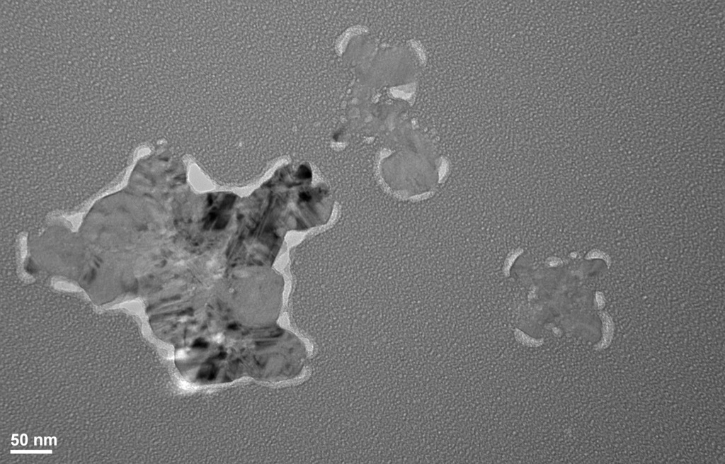
The TEM images capture the onset of silicon crystallization as well as the pore formation. It clearly shows that the silicon crystallization is accompanied by pore formation. Those silicon crystals are surrounded by pores, which is very similar to the ‘pearl necklace pattern’ Dave found before. In other words, the formation of pores helps to reduce the free energy during silicon crystallization process. I took some HRTEM of those silicon crystals.

The HRTEM shows that the pores work as boundaries to separate the amorphous silicon and silicon nanocrystals. The diffraction image prove the presence of silicon nanocrystals. A even closer look on the pore edge reveal the amorphous nature of this boundary. This might be a clue for the reamorphization phenomenon.

In sum, pores with irregular shapes and big sizes are formed in NSN stacks in FA condition. The porosity increases slowly with annealing temperature. The average pore diameter and pore density barely change while the pore roundness increases rapidly with annealing temperature.