I’ve been gathering data for a paper using my microporous MgF2 nanomembranes so here are some sample figures for such a paper.
Herein, we are trying to create a porous, Raman-compatible substrate for use in cell culture. Researchers have used Raman microspectroscopy to perform quantitative non-invasive measurements of biomolecules in cells. It’s a very exciting technique. While silicon based substrates have excellent properties for cell culture, they have strong Raman background signals and absorb a lot of laser power at the illumination wavelengths we would like to use. MgF2, Quartz, and CaF2 are considered Raman-compatible for their substantially weaker backgrounds. Researchers currently deposit or culture cells on non-permeable coverglasses made of these materials. However, we have known that cells sometimes require a permeable substrate to adopt morphologies that are more consistent with in vivo studies of morphology. So using our microporous nitride substrates, we wish to create a substrate that will have both the permeability and the Raman-compatibility necessary to facilitate more accurate Raman studies of those types of cells.
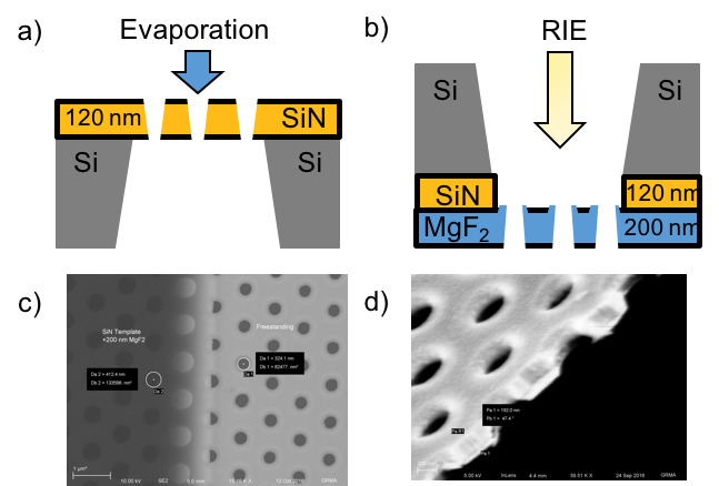
Figure 1. MgF2 nanomembrane material properties. (a)-(b) MgF2 relief pattern transfer, with cartoon crossections of microporous films (not to scale). Beginning with a freestanding film of microporous silicon nitride (a), MgF2 is evaporated onto the substrate (200 nm, 0.1-0.3 nm/sec, 250 °C, Platen Rotation), coating the porous substrate, resulting in a hybrid material. (b) The substrate is then inverted and purified using RIE (90% CHF3, 10% Oxygen, 75 mTorr, 100 W), releasing a freestanding nanoporous film of MgF2. (c) A SEM image normal to the membrane plane shows the infilling effect of the direct evaporation process, as the template pores narrow from their designed 500 nm diameters to approximately 325 nm. (d) SEM crossection of a partially etched MgF2 nanomembrane (with some template backing remaining), showing film thickness close to the targeted 200 nm.
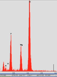
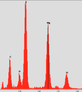
EDS measurement of the composition of the freestanding membrane. While the Mg and F signals are preserved across the freestanding region, the Si signal is not. The membranes are >85% MgF2 in the freestanding region. As a side note, there was some sample drift, so the image is blurred. This is a 30kX image.
Before Etch
After Etch
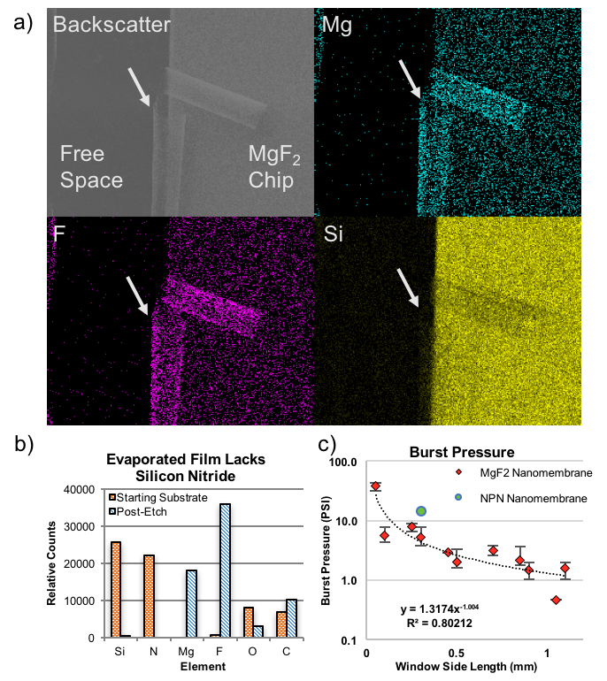
Previous Figure with 50 nm thick nanoporous MgF2. Here the burst pressure for the 200 nm microporous MgF2 is about 7 PSI, over a 5-slot structure instead of a square window.
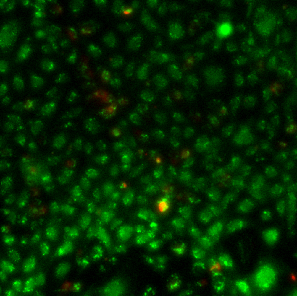
20X Live/Dead stain image of P6 HUVECS (Day 7) on fabricated microporous MgF2 grown in MCDB131 media. Eventually, we will use ARPE-19 Cells with tight junction staining which have a characteristic response to permeable substrates.
We will have to reestabilish the Raman background of the membranes, but the material composition looks to be the same as with my nanoporous material. HUVECS seem to stick ok without using any additional coatings.
Scott Russell from Mech. E. and Steve Gillmer came over to help Sarah and I try to record the burst of membranes at up to 2000 frames per second. Generally we used 100o frames per second because it was the best compromise between our ability to time the 1 s recording time and the amount…
This week I set up some diffusion experiments with the inner membranes of wafers 187 and 310. From the TEM images posted previously, we see that these inner membranes have what appear to be either very small pores or small divots that do not pass entirely through the membrane. I allowed the protein standards to…
This post shows that C-dots are pretty close to neutral. Here I’ve looked at gold nanoparticles and albumin. 5nm Gold: The distribution is very spread out, but everything centers around -58 mV. 10nm Gold: This sample looks a little bimodal. Peaks are at -33 and 0 mV. Albumin: Much better than the gold samples. It…
I would like to share a collection of high resolution SEM images of nanopores of polycarbonate track-etch (PCTE) membrane. These nanopores have very high pore length-to-diameter aspect ratio of 6000 nm / 25 nm. I hope you find them useful. Cross-section of PCTE membrane Cross-sectional view of long and straight nanopores with a close-up at…
While JK has been processing backside images from 50 nm, 75 nm, and 100 nm membrane SEM images for pore information, I thought I’d take a look at a 100 nm membrane from both the front and the back at the same spot. Here are the images referenced to a corner of the trench. The…