Are those pinholes or micron-size pores?
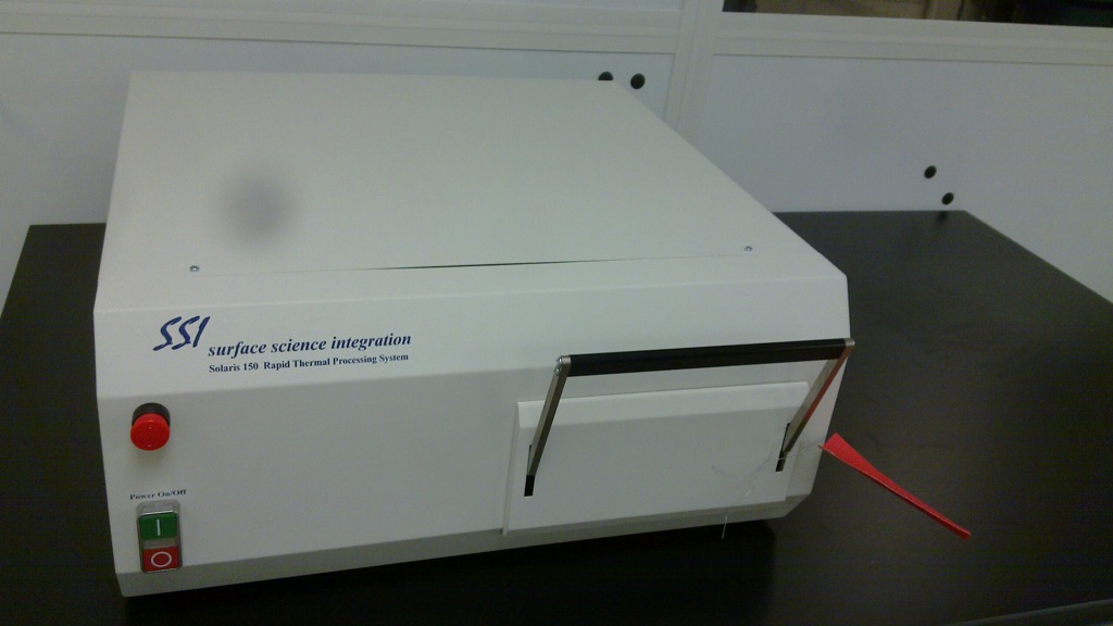
Hello everyone! After a long time waiting and setting up, the new AJA and RTP at Vanderbilt University now are ready to go! Here are a couple of pictures of the new AJA and RTP.
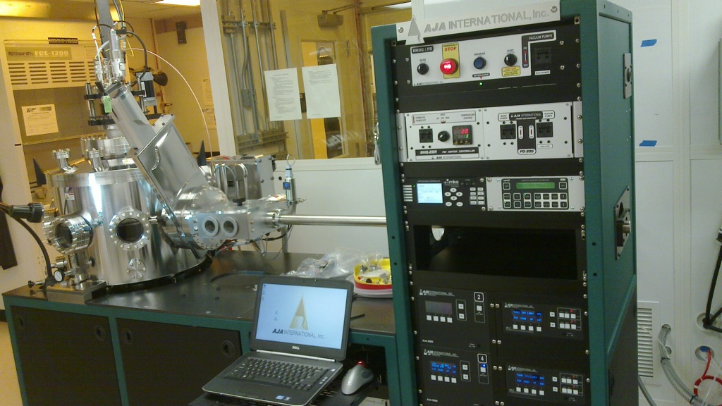
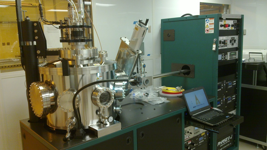
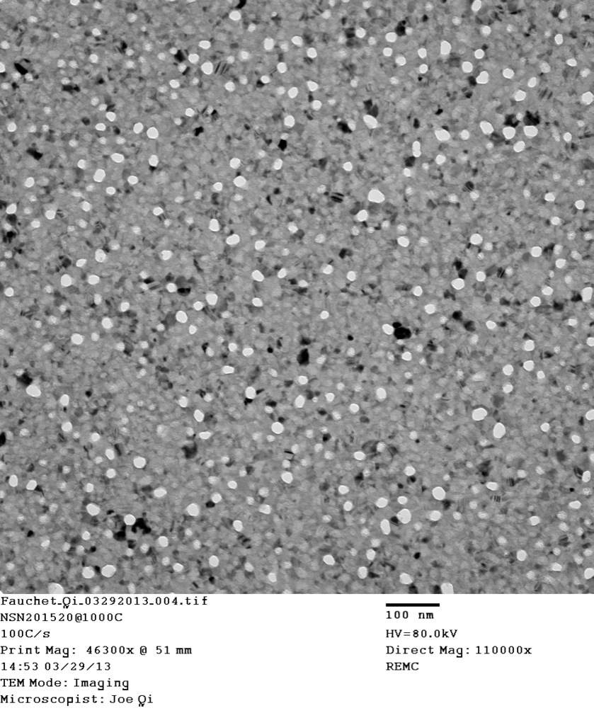
I have been working on testing the new AJA for a while with my old recipes. The new AJA system has a larger chamber (22″) and higher flow rate (30sccm max) with a bigger turbo pump. The results I got from this new system are different from our previous ones. The porosities and pore size from both the OSO and NSN stacks are lower than the numbers from the old AJA. The silicon film is 15nm thick and the oxide and nitride films are both 20nm thick. They are both annealed at 1000C for 1min with a 100C/s ramp up rate. The first result is from the OSO stack.

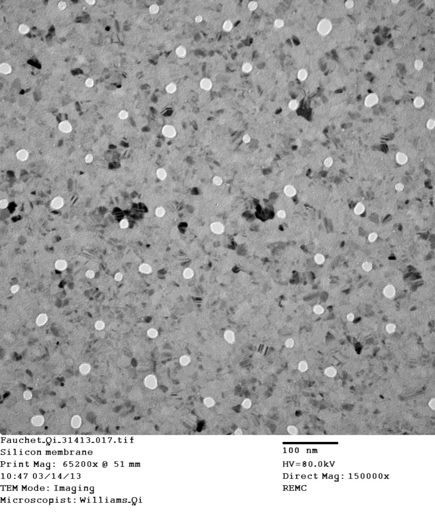
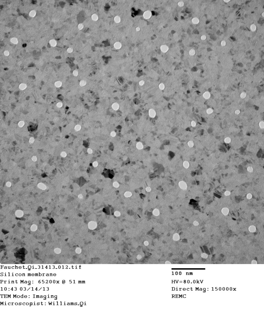

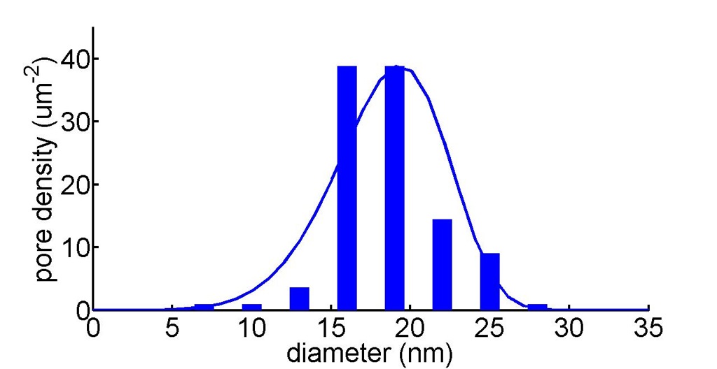
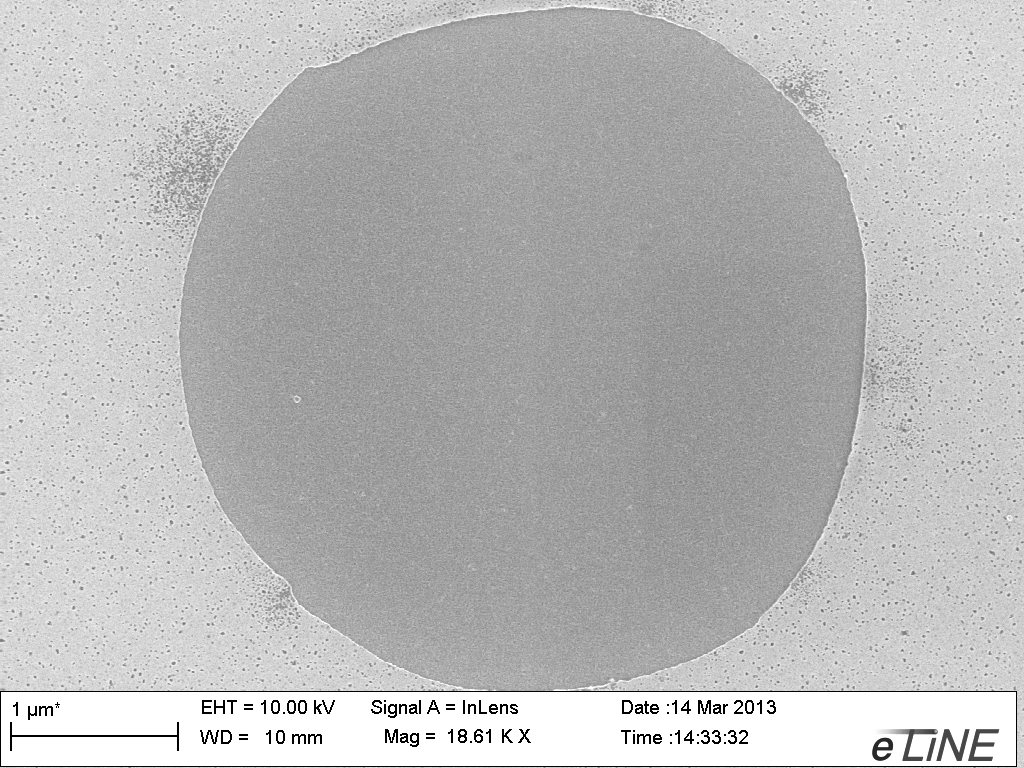
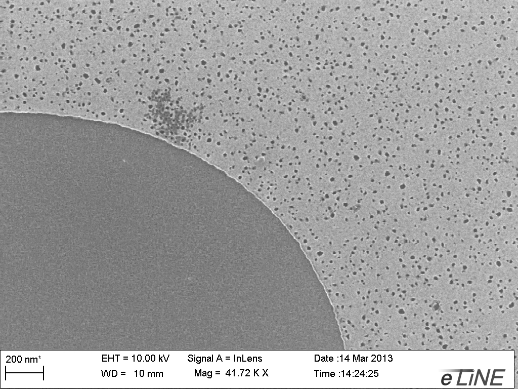
The porosity of this OSO stack is around 3% and the average pore diameter is around 18nm. The following is the pore distribution plot. Compared with the old AJA system which produced around 13% porosity and 23nm pores with the same recipe, the new system hasn’t optimized at current condition.
The NSN stack, however, shows very interesting results. Lots of micron-size pores show up after annealing in the silicon film.
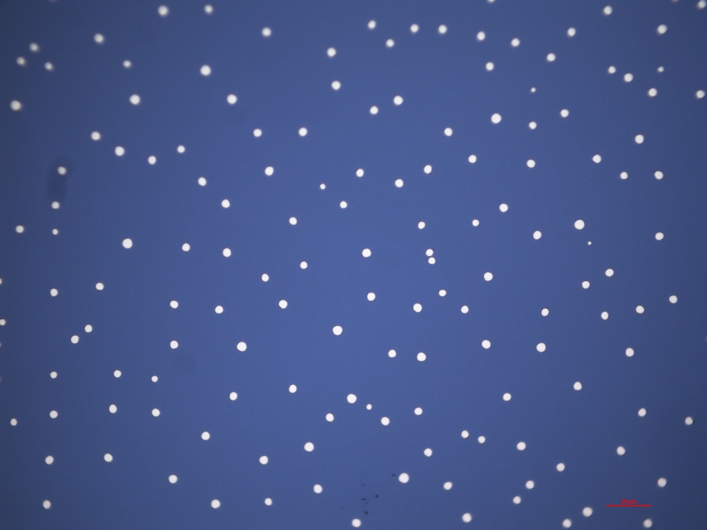
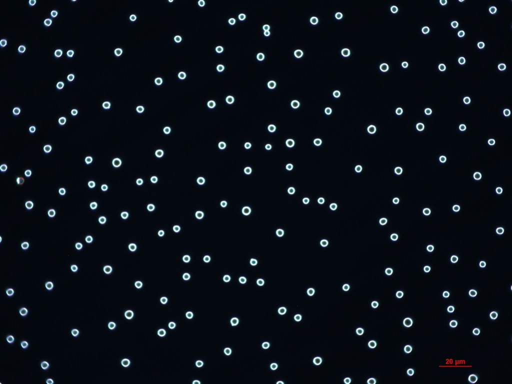
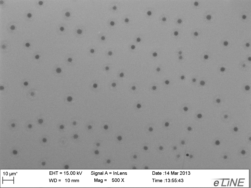
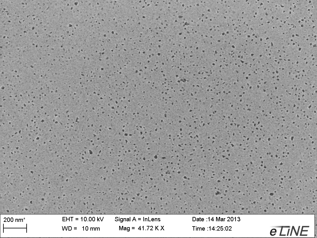
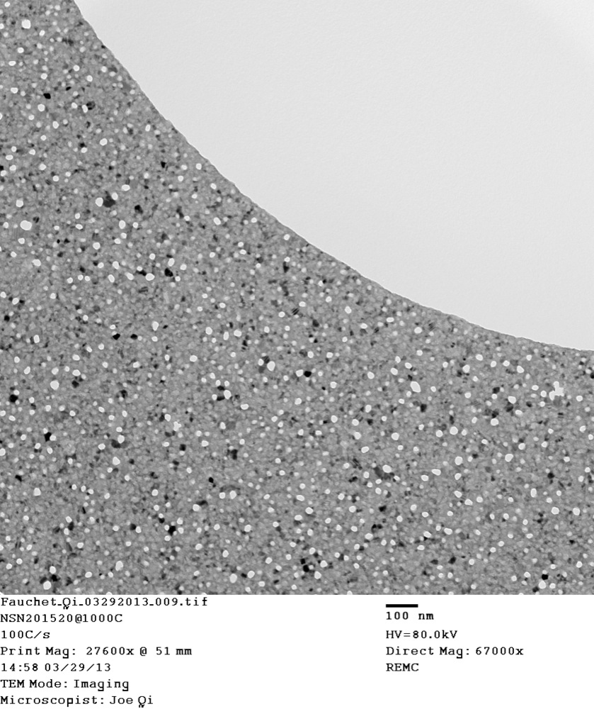
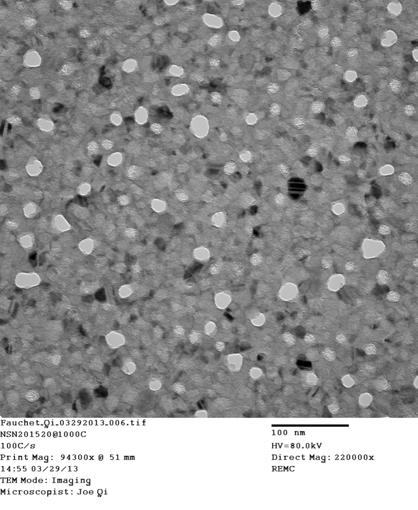
The top two are bright and dark optical images. Large density of pores with size around 3 mincrometer in diameter shows up in the silicon film. From the following SEM and TEM images, nanopores also appear in the silicon film. At this point I am not sure whether those micron-size pores are pinholes or not since the OSO and NSN wafers were deposited consecutively and there are no micron-size pores show up from the OSO stack.
Anyway, we are able to produce pnc-Si from this new AJA system and the old recipes need to be optimized in this new system. Another good news is that the new FEI Ossiris TEM is setup and we should be able to do some in-situ TEM annealing experiment pretty soon. Also a collaboration project about laser crystallization of OSO (NSN) stack with Oak Ridge National Lab was approved and we may get some interesting results from laser annealing.
Hey Joe, Thanks for the update. Glad to hear the systems are working.
As for the pinholes, these look very similar to what you were getting with the NSN stacks deposited at UR. I saw those same “pinholes” (I think we called them blisters) with my deposited NSN stacks ( https://trace-bmps.org/data/2012/10/19/nsn-sepcons/ ). We only saw the pinholes/blisters over the substrate with the samples at UR, presumably because we performed the EDP before the RTP.
Were the samples you show above etched in EDP before or after the RTP?
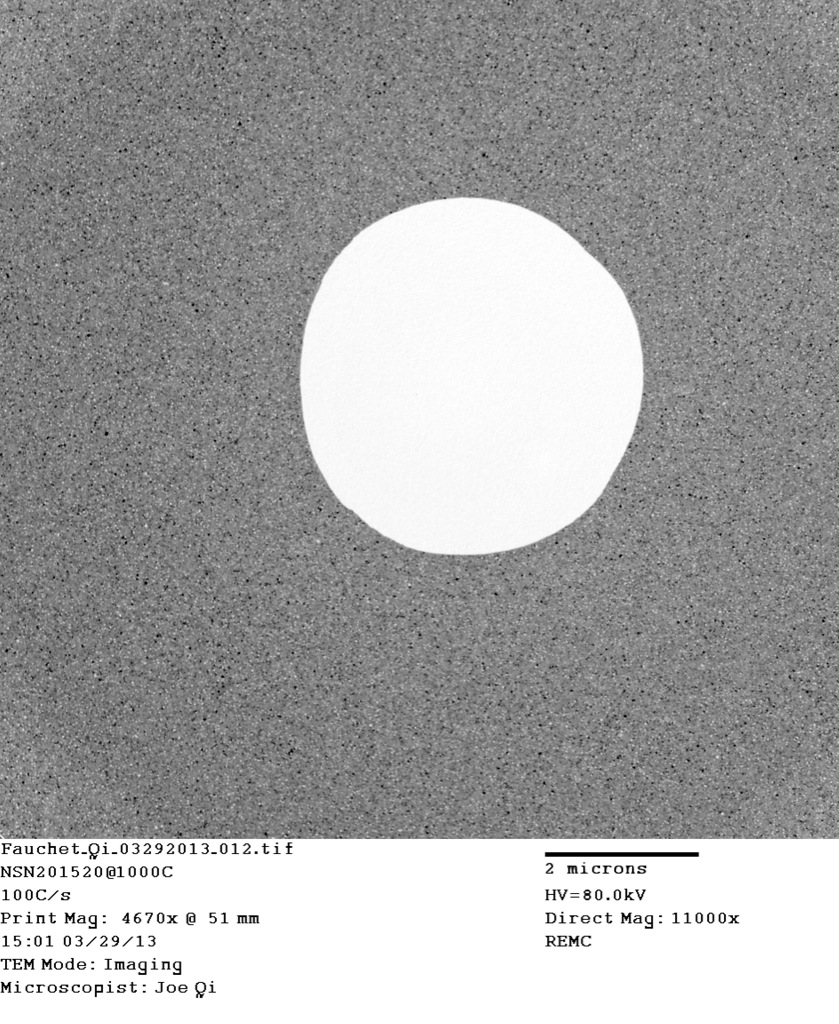
Hey Josh,actually I didn’t etch the wafer. I was using a single-side polished wafer for the deposition and then rtp the wafer. I lift-off the membrane for TEM image. That’s why I’m not sure whether they are pinholes/blisters since there is no EDP etching.