Critical Flux Control Experiments Across Three Different Wafers
Hi everyone, this is a short post quickly detailing some interesting quirks of different wafers as their respective chips are subjected to a control experiment (1x PBS, Qs = 30 ul/min, Qu= 10% Qs every 45 minutes).
First, lets look at 1256 (2.7% porosity, avg. pore diameter 33.2 nm).
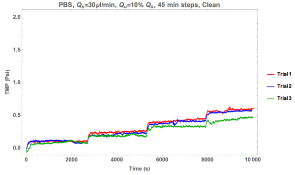
These results are a nice baseline that were acquired from the previous set of experiments I conducted.
Now 1292 (6.6% porosity, avg. pore diameter 44.3 nm)
I used two different bottles of PBS just to make sure that there wasn’t any contamination, the first graph shows an “old” PBS source (~1 month old, stored at 7 deg. C) and the second shows a “new” PBS source (autoclaved, newly opened, stored at 7 deg. C)
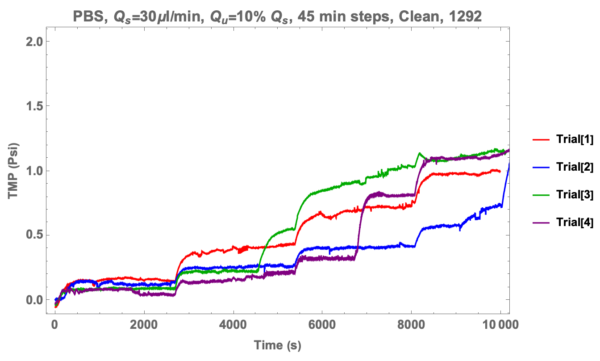

Interestingly, results are all less consistent than the lower porosity chips and the transmembrane pressure is actually higher! This shouldn’t be the case, and may be due to how the wafer was etched.
Luckily for us this has implications for the sensitivity of our wafers in the sense that we can potentially test to see how well etched our wafers are through control experiments.
Lastly, here’s data from 1297 (~20% porosity)
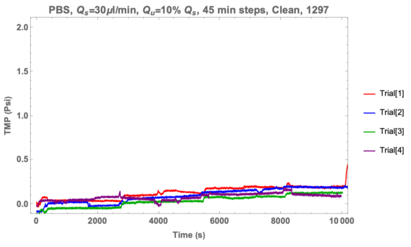
Flatter, and lower TMP than the 2.7% chips (as expected).