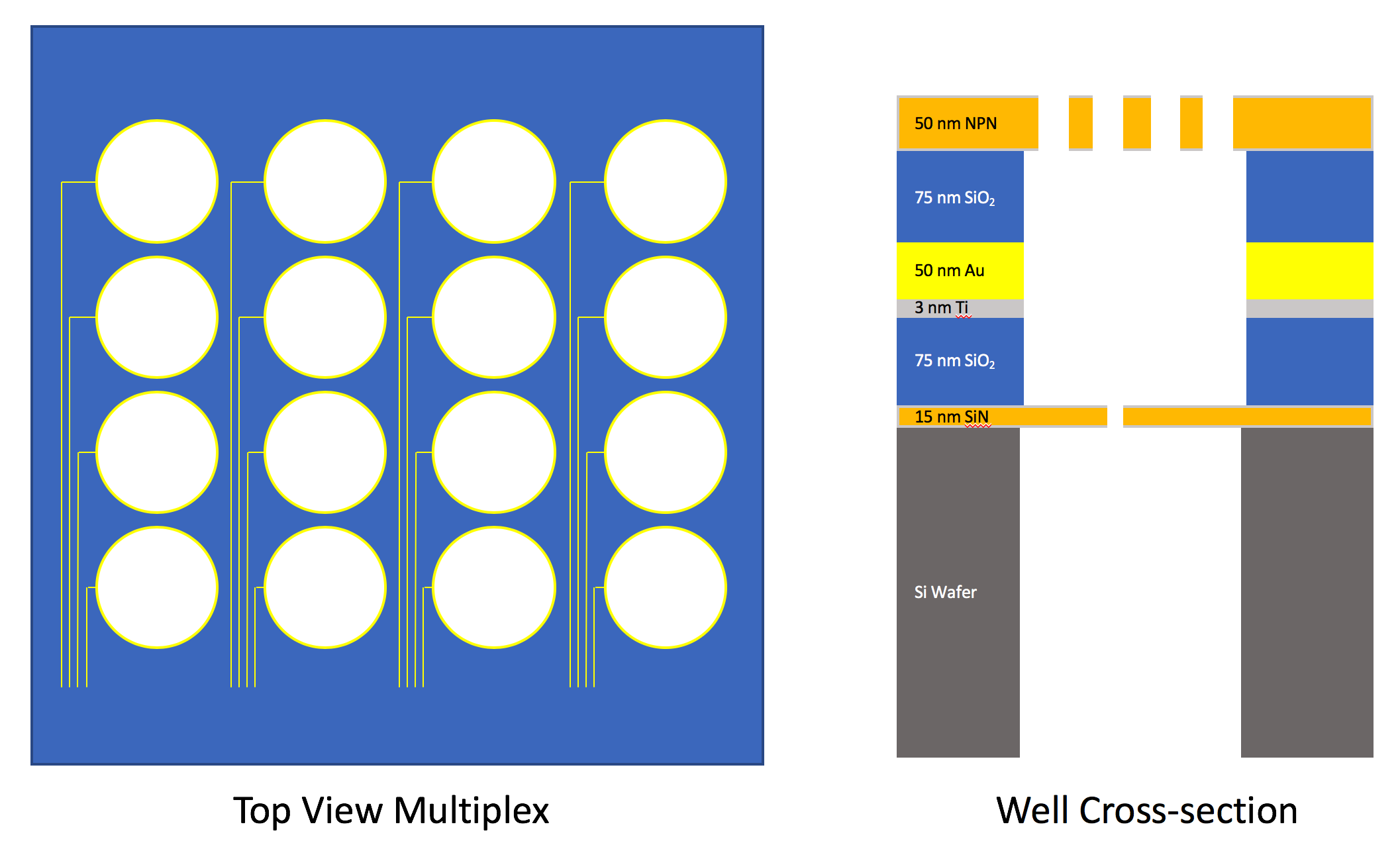
Preliminary Fabrication of a Tenting Well Oxide with a Buried Electrode
We want to create a structure that can more easily control the electric field inside of the Monolith cavities, by adding an electrode specific to each well. My solution is to create a hybrid film stack, replacing some of the SiO2 spacer with a gold layer that is in fluidic contact on the walls of the cavity.
Fabrication
With Alec assisting, I evaporated SiO2 at 150C (6KV oxide, 0.1-0.3 nm/sec, platen rotation, target 75 nm, 4-11 mA beam current, 5e-5 torr) onto a few NPN chips and blank Si chips using the Kurt Lesker PVD-75B. After this step, I sputtered Au onto the substrates without removing the chips from the tool, using a recipe that I created for SERS work (50 nm, 200 W, Ar plasma). The substrate had cooled down to about 90 C at this point. I then removed these chips from the tool, after cooling to 70C, because another user needed to use the tool. I came back shortly thereafter, and reran the SiO2 deposition on the SiO2-Au coated chips, completing the process.
Analysis


Future Work
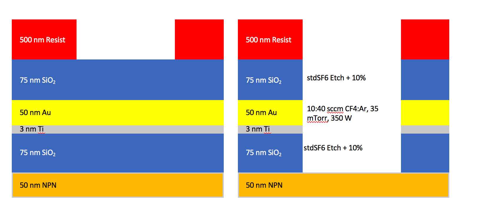
With JK’s help, I have a microhole patterned in photoresist on top of this stack; now I need to transfer the pore pattern into the film stack using a variety of RIE chemistries. I intend to etch the glass using my standard SF6 recipe, then ‘sandblast’ the thin Au layer using a 350 W Ar plasma, and finally use the SF6 recipe again to get through the remainder of the film stack. It remains to be seen if the photoresist will hold up against this strenuous level of etching. I will also throw in Au coated chips alone to see if the etching is any different.