Early results with monolith devices
I have had a chance to play with some of the chips from Lot 1278, specifically the design with the 2 micron slots. Results are a bit of a mixed bag.
Wetting these chips continues to be a challenge. My first attempt to use the vacuum wetting protocol in ethanol resulted in a broken membrane, suggesting that the long aspect ratio weakens the membranes compared to the microwell design. This can be mitigated by breaking the vacuum slowly.
Once membranes breaking was dealt with, I had a new problem: every pore I made had extremely high low-frequency noise, which renders pores useless most of the time. In addition, I observed several pores apparently dewet themselves in the middle of fabrication, which looks like the image below, in which the tunnelling current suddenly drops to zero:
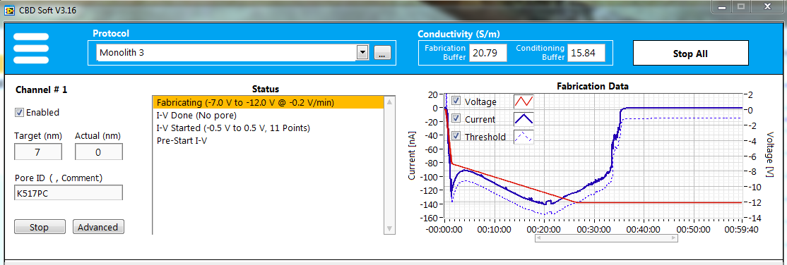
I believe we can explain both of these observations using some other results we obtained a while ago. When ethanol is mixed with water, the gas solubility of water is so much lower than that of ethanol that bubbles immediately form in the mixture. I believe that when we use ethanol under vacuum to wet the cavity, we end up trapping bubbles inside the cavity when we switch over to an aqueous solution. Bubbles have been pegged as a cause of low-frequency noise in nanopores, and the movement of a larger bubble through the cavity could potentially explain the apparent dewetting which I have now seen twice.
This seems to be at least partially addressed by using a degassed mixture of water and ethanol to do the wetting instead of just pure ethanol – since switching over to this new solution I have had more success with low-noise pores.
So far I have gotten DNA through 4 pores of an attempted 8. Of those 4, two had very high noise and seemed to have pre-existing defects in the membranes. I managed to get DNA through anyway, though the results are not particularly useful for comparison to the Nano Letters paper since whatever mechanism causes the low-frequency noise also seems to affect DNA translocation kinetics, making events sticky and take longer than one would expect. Of the remaining two, one of them showed channel gating, in which there were two different open channel current states, of which it spent most of its time in the lower conductance state. This pore also showed longer, sticky-looking translocations and without knowing what caused the gating I can’t do much to interpret those results.
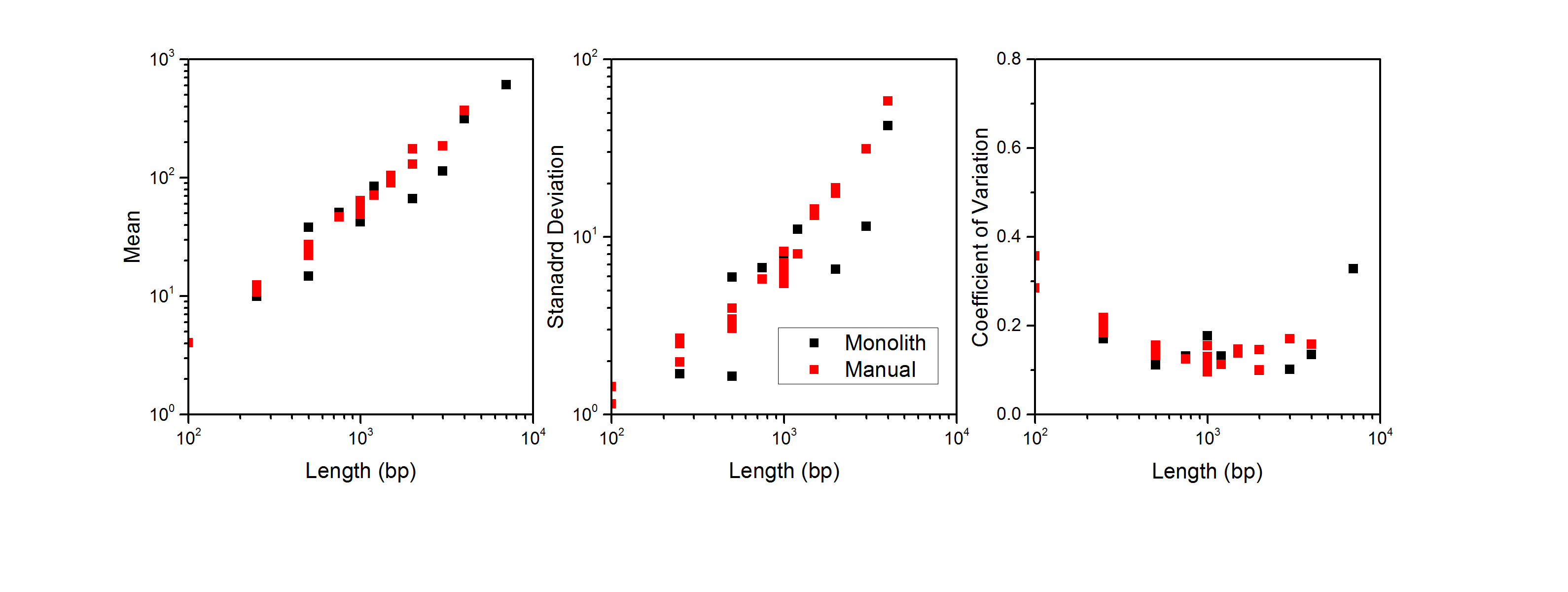
The last pore gave me excellent results. I was able to run the full range of DNA lengths on the pore one after the other. The noise was reasonable, and capture rates were good. Below, I show the mean passage time, standard deviation, and coefficient of variation for this device (black), overlaid on the data from the Nano Letters paper (red).
NOTE: The below plot is in error, due to a misplaced bracket in one of my calcations. The corrected image is below.

Corrected image:
A possible issue with these chips is something that we probably could have anticipated: because the NPN only has actual through holes in the central region of the cavity, it is entirely possible that the sensing pore is made off-center, below an area which has no NPN pores directly above it. In fact, from the images I saw on Basecamp, this is the most likely outcome if we assume a uniform probability of forming the pore anywhere on the sensing membrane, since the overetched region has a larger area than the part of the NPN that has through-holes. With the sensing pore far from the NPN, all of the benefits to the passage kinetics are lost since the molecule can relax in transit between the NPN and the sensing pore.
This leave the question for you guys: is there a process by which either overetching can be reduced, or by which the NPN pores above the overetched region could be opened after the fact without damaging the portion that was already open?
I am able to wet inside the cavity, I am able to fabricate sensing pores, and I am able to pass DNA through the system just like in the Nano Letters paper. Clearly the process you have developed works as intended.
1. is there a process by which either overetching can be reduced, or by which the NPN pores above the overetched region could be opened after the fact without damaging the portion that was already open?
I’m not sure about reducing the overetch from the XeF2, but we do have a way to open up pores more in localized region. I can pattern a photoresist on top of the monolith (see Alec’s post https://trace-bmps.org/cell-morphology-and-neutrophil-transmigration-on-microporous-npn/), and then partially etch the pores to blow them out relative to the rest of the pores. Even a small 1.2x increase will create a 1.2^4 = 2.07 increase in conductance. As a bonus, the etch gas may diffuse underneath in the cavity and weaken the ssNP right below the pores that are being etched. Basically, by locally controlling the pore size with additional etching, we should be able to preferentially place self-aligned pores.
I’m not sure I follow. Which pores are being partially etched? It’s not that we need more conductance, it’s that we need NPN pores to be essentially everywhere that the sensing membrane is exposed, so that no matter where the sensing pore forms, there will be NPN pores directly above it.
thanks for the update.
Re pore misalignment: An alternative strategy would be to pattern the sensing membrane, by locally thinning it below the NPN.
Re lack of improvement in dynamic of passage: Could it also be that the NPN pore size/porosity is such that the DNA is not confined in the gap or NPN pore (e.g. NPN pore is 200nm)? Could it be that the NPN is cracked? can the device demonstrate trapping to confirm it is not?
QUESTION FOR SIMPORE: WHEN CAN WE EXPECT A NEW BATCH OF MONOLITH DEVICES? CAN WE DISCUSS THE DESIGN TO MAKE SURE IT IS MADE TO SPEC (gap height, etc…)
Unlikely that the NPN pore size distribution is so different from previous iterations. These devices with the slits are probably not good traps because of the extra dimension in which to escape, so escaping polymers would not confirm cracking for this design.
I think we can make the sensing pore appear by preferentially weakening the ssNP in parts below the pores. Thinner membrane creates more likely breakdown:
Problem now: https://trace-bmps.org/wp-content/uploads/sites/3/2018/06/Screen-Shot-2018-06-26-at-12.50.17-PM.png
Solution Proposed: https://trace-bmps.org/wp-content/uploads/sites/3/2018/06/Screen-Shot-2018-06-26-at-12.50.39-PM.png
I see, that could work, or at least increase the yield. Just in case you haven’t seen it yet, here is our paper on more or less this process: https://www.ncbi.nlm.nih.gov/pmc/articles/PMC5408306/
Thanks, I hadn’t read this one yet, but I guessed as much based on our conversations. Natively CHF3/SF6/O2 RIE won’t be inducing any defects, but we could try to add a few broken points with an Ar plasma addition to the etch gas. There’s probably a gas combination that could expand out the membrane up top without eating too much material in the bottom. After all, it is only 15 nm of material to work with.
I see that multiple pore formation might occur. With a lack of strong defects from the He mill, I think this is less likely, especially as the thinning will be localized to where the pores are open. I use low-pressure plasmas, so I think the directionality should be good.
If we go this route we could use a much thicker SiN membranes for the sensing membrane – make it 50 nm or even more, and then etch down to ~10-20 nm only right under the NPN. This might make the whole process easier since the SiN would be that much stronger.
All monolith chips that Vincent’s lab has received thus far were produced from the same batch of wafers on which the film stacks were all deposited at the same time. The new set of chips just delivered had the same spacer thickness as previous sets of chips so were potentially mislabeled. We are planning to send wafers out next week for a new set of film stacks so can have Vincent’s folks check out those specs. The quote is on BC under the R21 project from the film deposition vendor with the thickness of films in the stack.