More Negative Data for the Nanofluidic Transistor
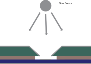
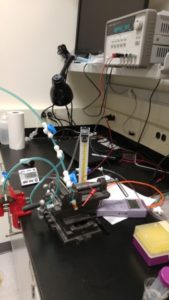
I don’t think I ever posted it on the blog, but two years ago I discovered something neat. At the time, I was trying to make my nanofluidic transistor, and I was reading Marina’s thesis. She tried to improve the efficiency of our EO pumps by putting silver films directly on the front and back of the chip. I don’t think the effort went very far, probably because it turns out that it’s really really hard to put two separate metal films on the front and back of our chips and not have them touch through some of the pores. But at the time, I was learning to use the E-beam deposition system and I thought I’d give it a shot. I coated the front of an NPN chip with 3 nm of Ti and 12 nm of Ag, and then flipped it over and did the back side. Then I devised a little test setup that looked something like this:
![]()
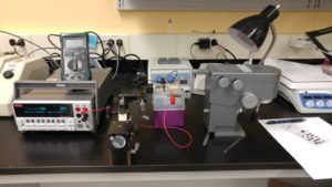
I used the two micromanipulators to press two silver wires to various points on the chip, and measured the resistance between the points.
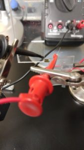
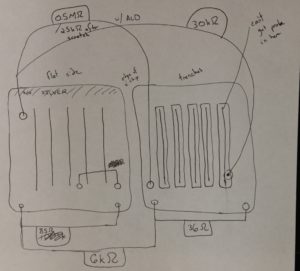
Note that the setup was precise enough that a couple of times I was actually able to make contact with the 10 nm thick alumina layer on the surface of the chip without actually punching through to the silver layer below it, which is mind boggling:
I found that the resistance across the surface of the chip was about two orders of magnitude lower than the resistance from the top to the bottom of the chip – it seemed like a real success!
But then Josh Winans sat me down and explained once again that if you think you got something science-y to work the first time, you’re interpreting your data wrong.
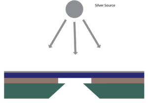
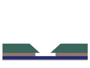
Here’s a view of the process flow (not shown is 10 nm of conformal, gas-based ALD-ed alumina deposited last of all):

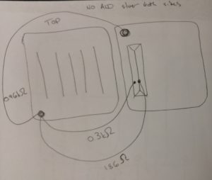
So the front and back of the freestanding NPN don’t have to be electrically isolated for the front and back of the chip to be. But this actually could be useful for us. Consider the following: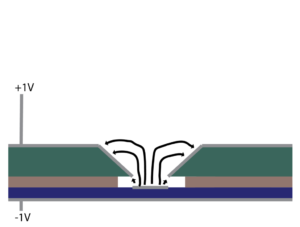
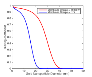
We could use these two films as the two electrodes needed to make a nanofluidic transistor. We can pump charge into the membrane through the top of the chip, with respect to the bottom of the chip, and the field should propagate out along the rough field lines I’ve drawn and change the pore-particle interactions. My sieving model predicts that if you can change the surface charge of the membrane by 1 V, the curve will shift quite dramatically:
Chip with pore diameter of 47 nm –
Chip with pore diameter of 27 nm (47 nm with 10 nm alumina ALD) – 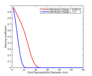
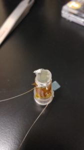
So I made some of these chips. 3 nm Ti, 12 nm Ag in the e-beam deposition system in URNano. I characterized them using my micromanipulator setup, and saw the behavior we expected.
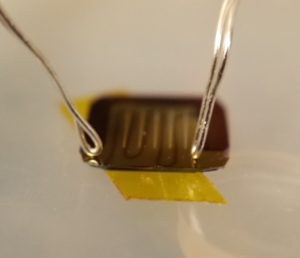
(Note – the above is actually one of my ACEO chips, but the setup was the same).
Using an even thinner probe, I think I was able to actually touch the backside of the freestanding membrane without breaking it (although I can’t be sure that the act of measuring it didn’t break the membrane. It was hard to see what was happening at that scale). Also, that chip didn’t have the 10 nm insulating alumina dielectric that all the others had.
So, armed with these chips, I tried some separations:
I measured the sieving coefficient of 5nm gold, then switched to 15 nm gold. In neither case did I see any difference (by eyeball, I wasn’t using the Tecan to characterize these samples, but the change should have been super obvious) in sieving between -1V applied voltage and no applied voltage.