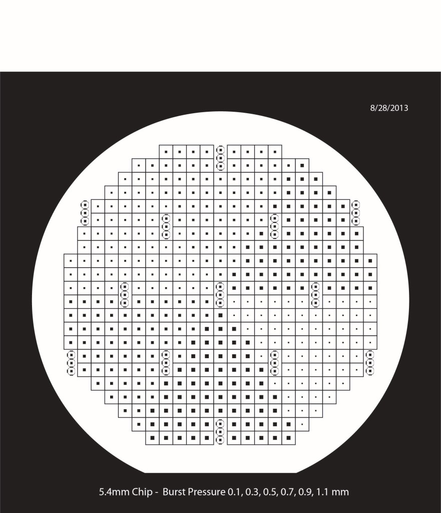
MgF2 Burst Pressure Analysis
Key Ideas
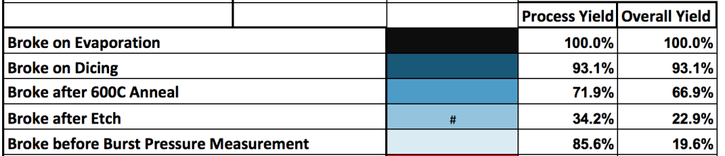
- I took a wafer with ~400 chips of varying square window sizes, ran my MgF2 process, and recorded the pressures it took to burst them.
- Overall yield was about 20%, most of them smaller windows. I was expecting ~50% based on my previous work. Variation in the etch step destroyed the yield.
- MgF2 nanomembranes are weaker than pnc-Si, ~25% as strong.
- MgF2 nanomembranes don’t follow the same exponential dependence observed for pnc-Si and NPN materials.
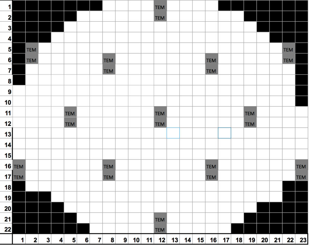
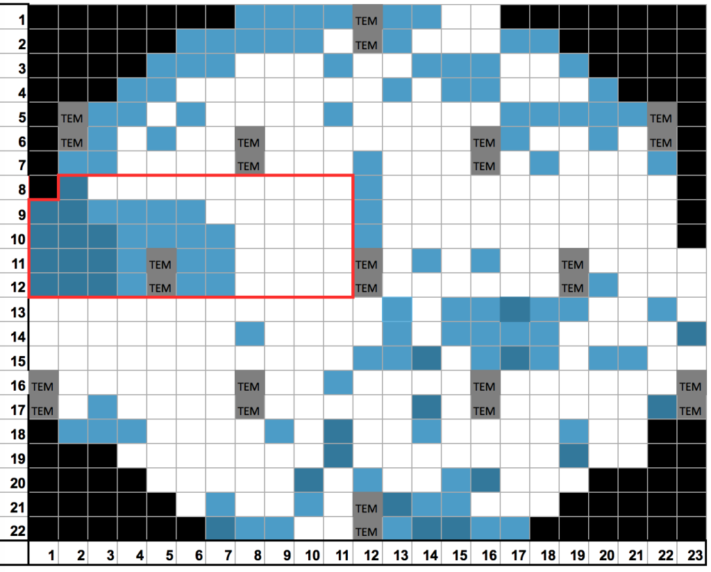
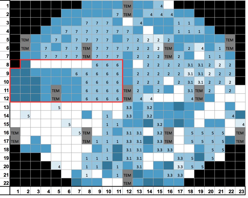
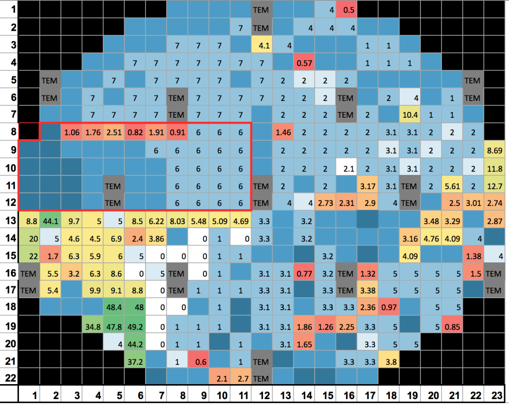
- Overall wafer yield summarized in a GIF (colored = burst membrane):

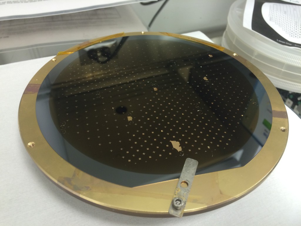
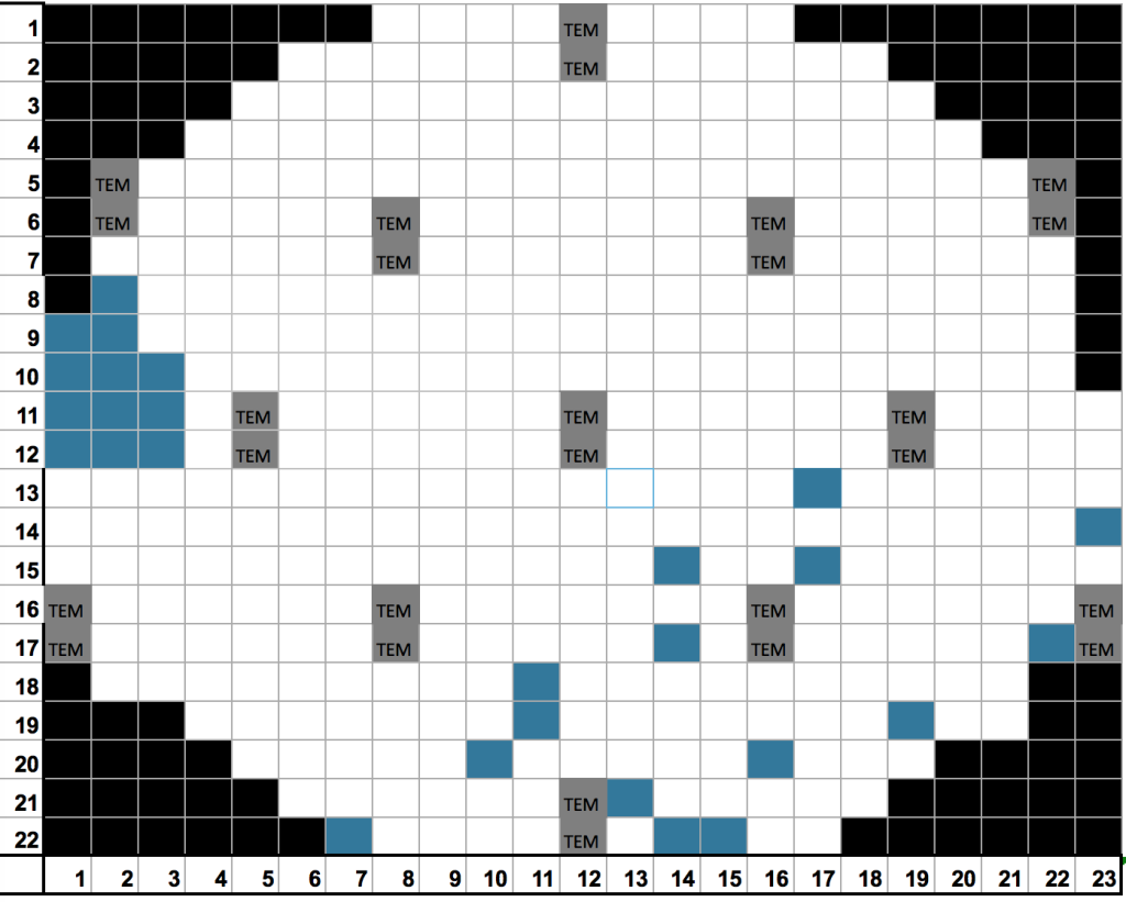
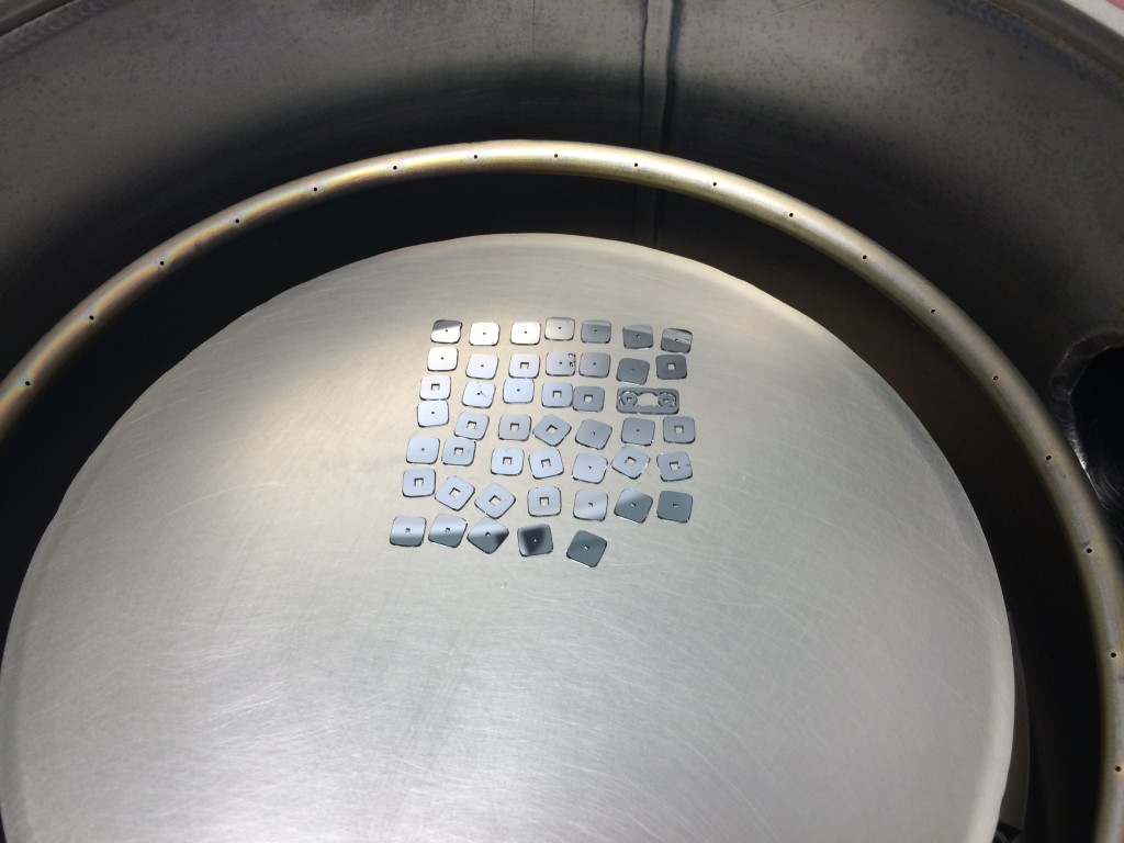
Initial Wafer

Deposition
Using the Kurt Lesker Sputter/Evaporator, I deposited 50 nm of MgF2 on my wafer. Base pressure was 5e-5 torr, and I used the 6 KV oxide recipe, with platen rotation on, at room temperature. I controlled the current manually, varying the current between 0.5-2.0 mA to achieve stable deposition rates. I tried to maintain a rate between 0.1-0.2 nm/s, but I occasionally had spikes up to 0.45 nm/s, unusual in this recipe. The coloration of the film was a deep purple, as I have noted before for this film thickness/substrate. No broken windows were observed at this point.

Cleaving
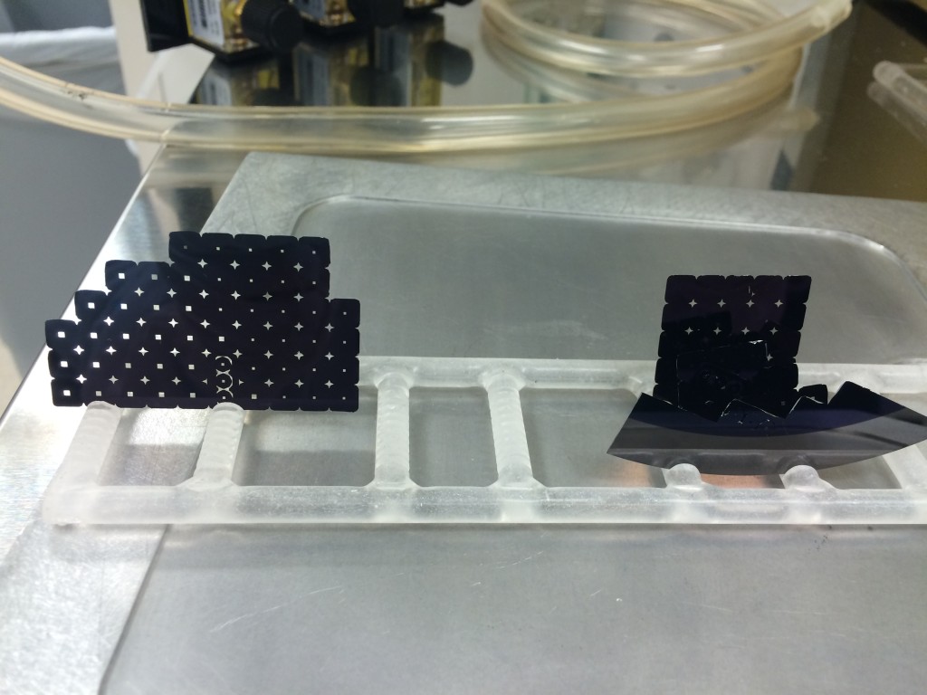
Sectioning the wafer into smaller pieces to fit into the 3″ tube furnace was nervewracking, but overall, I didn’t destroy that many chips in the process of doing so. The major crack I identified was in the bottom left quadrant, and my first broken chips came from there.
Annealing
I ran a 2 hr recipe to anneal the MgF2, in 15 sccms of Ar as an ambient. Insertion (t=0) occurred at 200C or below, and then ramped up to 600C. Removal (T=2.5 hrs) occurred at 450C or below. I lost the locations of a single large block of chips when it clipped the edge of the furnace. User meeting attendants know my consternation.
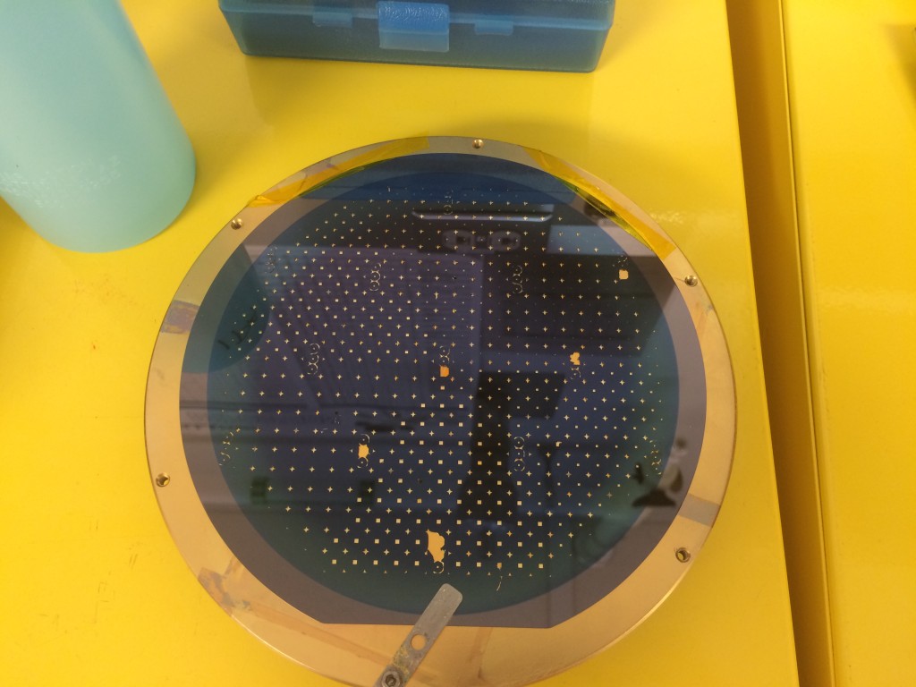
Etching
I flipped the chips over and removed the silicon nitride from the backs of the deposited films. My etch yields were terrible. I use a mixture of CHF3 and 7-10% O2 at 75 mTorr at 100 W. This provides an etch rate of 50-60 nm/min. I cleaned and seasoned the chamber each day with an Ar etch for 10 min, followed by a 60s etch using the above recipe, tuning in an acceptable run. I lost a great number of chips in each box with the 70 s etches, and the power spikes. To try and prevent time for the power supply to spike, I lowered the etch time to the absolute minimum to get rid of a nitride film. I was unable to find what was causing my plasma to spike wildly occasionally, and not other times. Box 7 had zero yield. At this point, I had not quantified a maximum power associated with broken chips. If 120W is a practical limit, I am operating fairly close to that power ceiling. I will have to see if I can make a recipe that is lower power, stable, and maintains the low etch pressure and gas ratios. The tradeoff would be potentially increased polymer formation and of course longer etch times.
| Box | Date | Pressure (mTorr) | Average Power (W) | Max Power (W) | Time (s) |
| 1 | 1/21/15 | 79 | 98 | 101 | 70 |
| 2 | 1/22/15 | 82 | 110 | 115 | 70 |
| 3.1 | 1/22/15 | 79 | 98 | 170 | 70 |
| 3.2 | 1/22/15 | 80 | 97 | 115 | 70 |
| 3.3 | 1/22/15 | 78 | 96 | 99 | 55 |
| 4 | 1/23/15 | 78 | 96 | 101 | 55 |
| 5 | 1/23/15 | 81 | 98 | 112 | 55 |
| 6 | 1/23/15 | 78 | 98 | 105 | 55 |
| 7 | 1/23/15 | 82 | 101 | 124 | 55 |
Burst Pressures
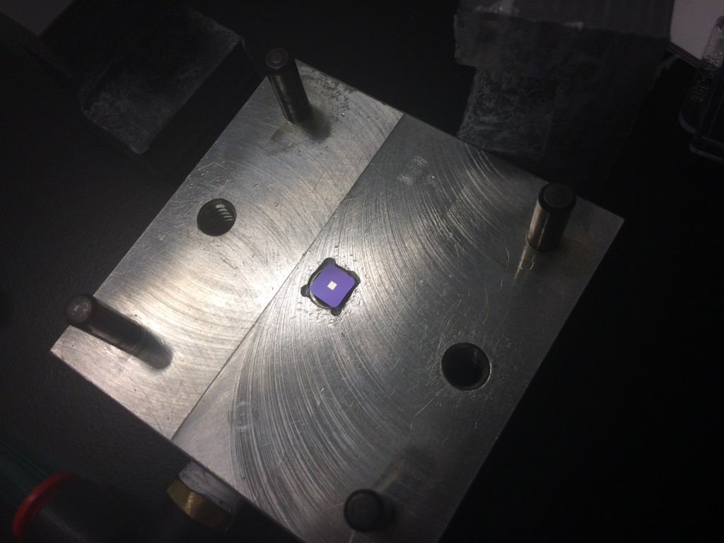
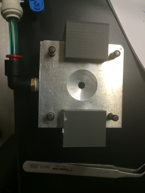
I then recorded burst pressures using the same setup as Sarah used in her work. Instead of screwing the chips into the clamp, I used a hard clamp to make sure the same pressure was applied to the chip everytime.
Analysis
| Window Size (mm) | Average (PSI) | Std Dev (PSI) | Count | Coef. Of Variation | Relative Yield |
| 0.10 | 15.42 | 16.20 | 36 | 1.05 | 55% |
| 0.30 | 7.78 | 4.22 | 7 | 0.54 | 11% |
| 0.50 | 1.43 | 1.55 | 5 | 1.09 | 8% |
| 0.70 | 2.99 | 0.91 | 15 | 0.30 | 23% |
| 0.90 | 1.50 | 0.67 | 6 | 0.45 | 9% |
| 1.10 | 1.76 | 0.94 | 12 | 0.54 | 18% |
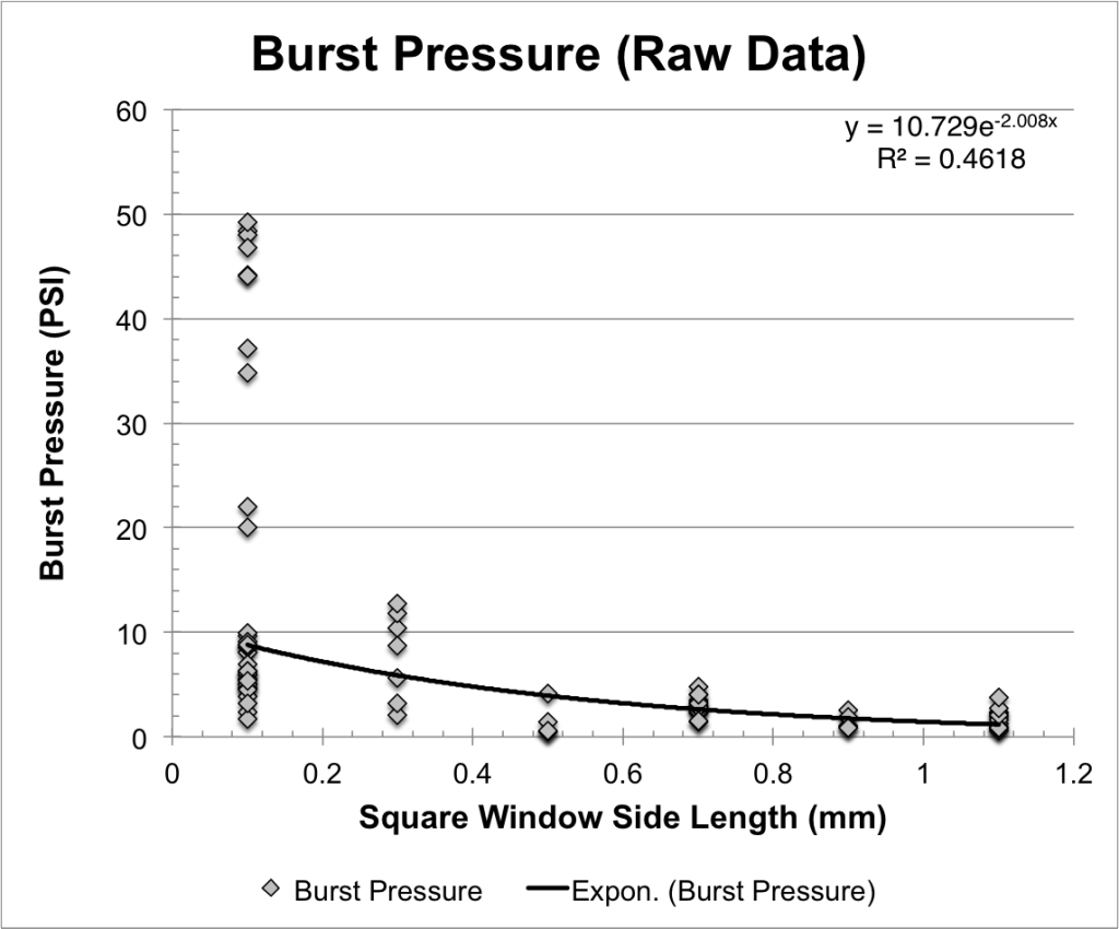
The graph includes everything that I measured, including the chips where the thickness of the film is unknown, but almost certainly occluded (blue ring). In order to get a more precise measurement of my process, I removed data points that were within 2 chips of the edge of the wafer. About half of the chips measured are thrown out. The coefficient of variation is reduced for a few window sizes, indicating a tighter distribution.
| Window Size (mm) | Average (PSI) | Std Dev (PSI) | Count | Coef. Of Var. | Relative Yield |
| 0.1 | 6.40 | 2.05 | 18 | 0.32 | 27% |
| 0.3 | 5.31 | 3.70 | 4 | 0.70 | 6% |
| 0.5 | 2.04 | 1.84 | 3 | 0.90 | 5% |
| 0.7 | 3.16 | 0.93 | 11 | 0.29 | 17% |
| 0.9 | 1.50 | 0.67 | 6 | 0.45 | 9% |
| 1.1 | 1.59 | 0.62 | 7 | 0.39 | 11% |
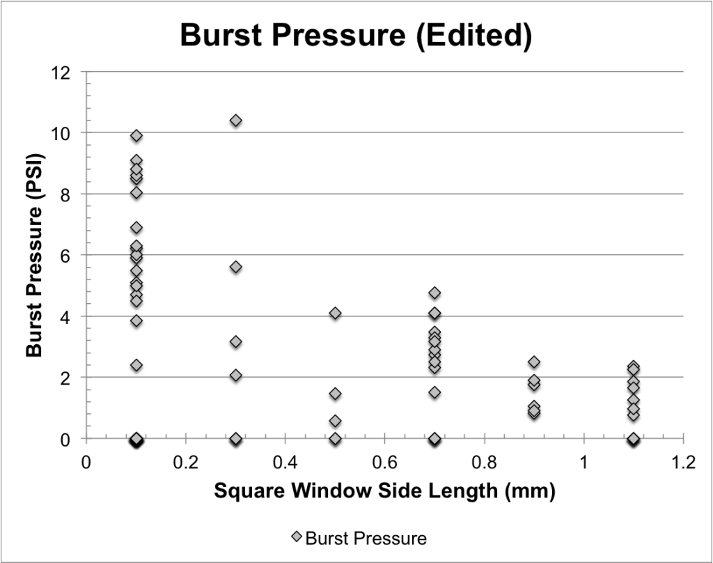
This whole graph would fit in the bottom portion of the first graph.
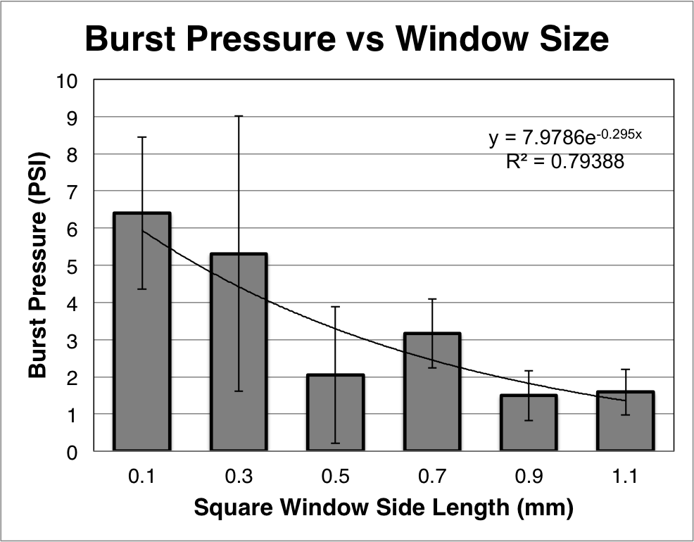
Compared to pnc-Si and NPN, the MgF2 is much weaker, only a quarter as strong as pnc-Si at the smallest window size. The power regression is broken here as well, with the exponent only being 0.6 compared to 1.2.
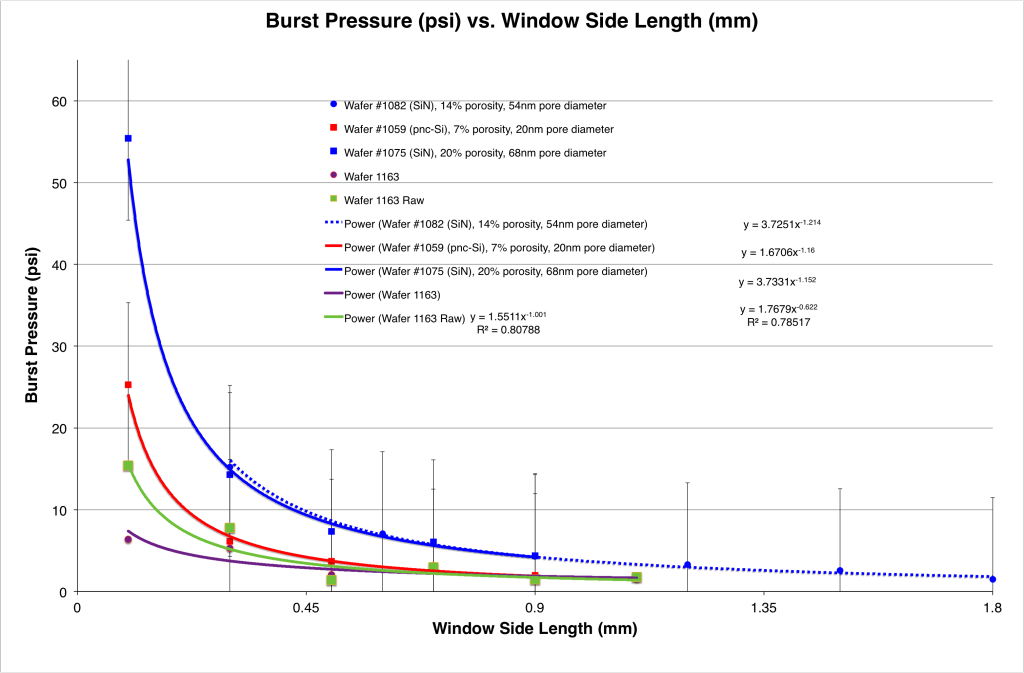
If we run another burst pressure wafer, we might get cleaner data from higher n. First I need to solve the problem of the etcher. Overall, this study reinforces what we’ve practically known for a while: my MgF2 nanomembranes are delicate. We have been able to grow things on them in vitro, but bubbles will wreak even more havoc on them compared to silicon materials.