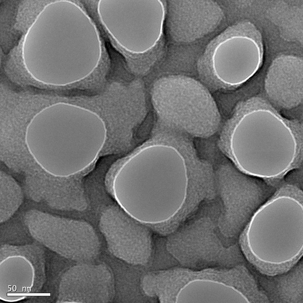
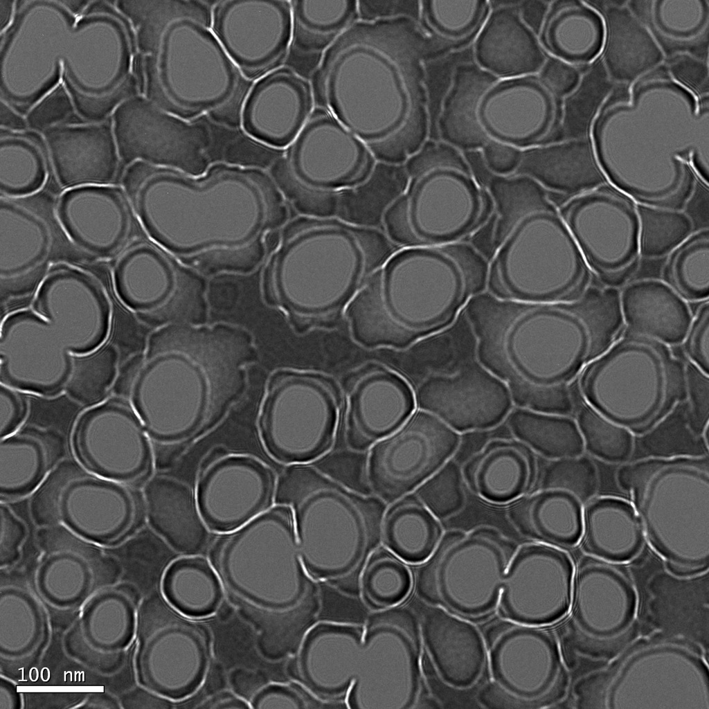
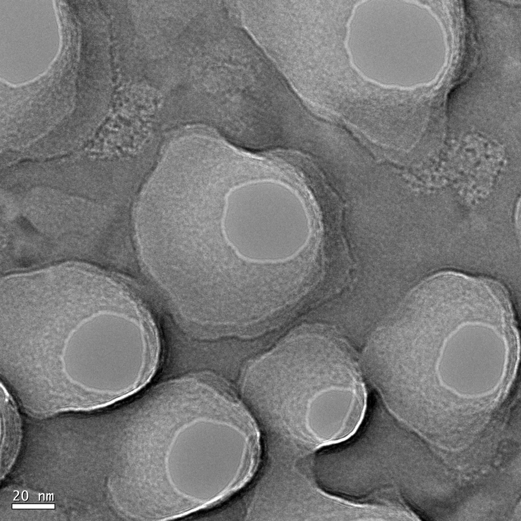
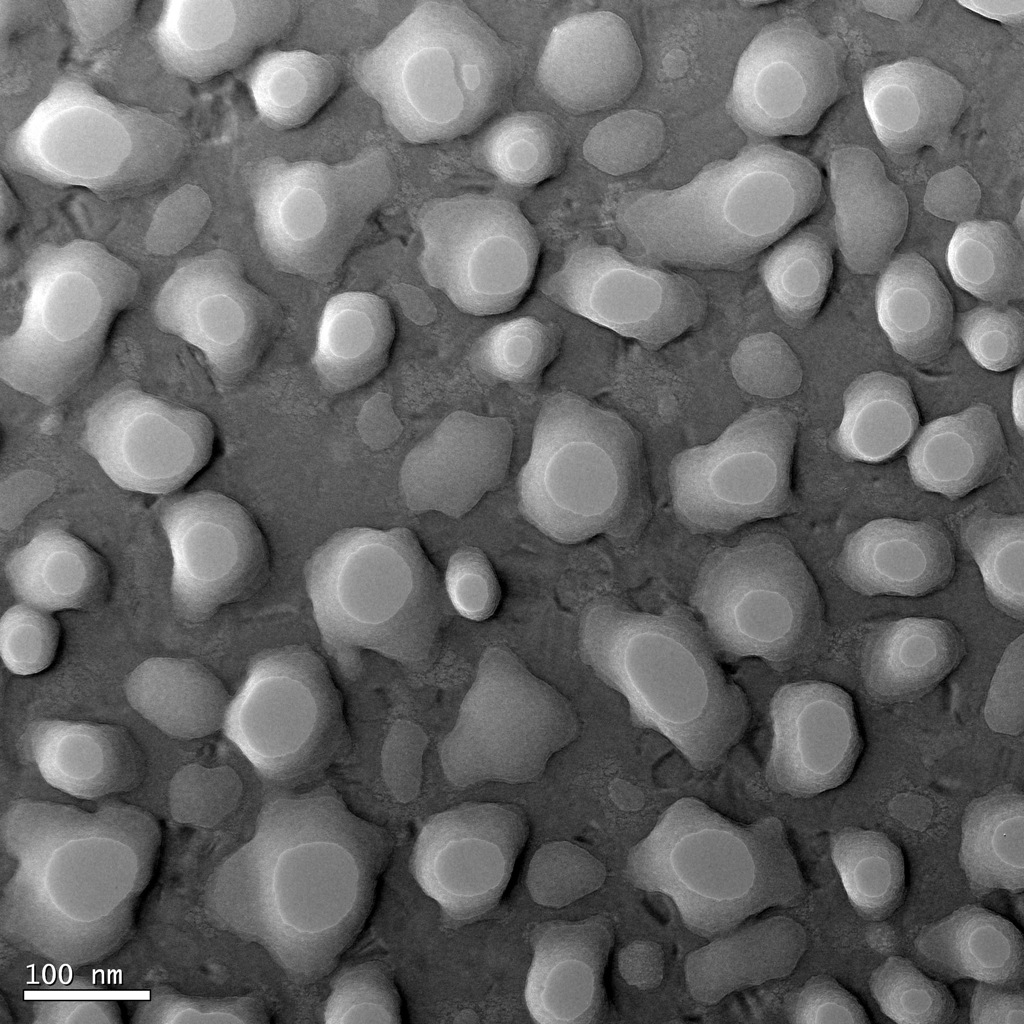
SiN NP wafer #'s 1029 and 1030 pore size revisions
Our work with permeance and hydraulic permeability tests on the SiN-NP seemed to show that the porosity and pore sizes I had calculated from the STEM images were too high. I used URnano’s TEM to get better quality images and, as suspected, the pore sizes need to be revised smaller.
Wafer # 1030 (40 s RIE) – ~26% porosity, ~58 nm avg. dia.
Wafer # 1029 (30 s RIE) – ~11% porosity, ~40 nm avg. dia. (calculated by measuring individual pores in ImageJ)
Wafer # 1036 (20 s RIE) – 0% porosity, 0 nm avg. dia.
Wafer # 1037 (10 s RIE) – 0% porosity, 0 nm avg. dia
Sorry for all the confusion. I’ve gotten a better feel for the STEM recently, and I might be able to get more accurate measurements in the future, but I will probably use either Karen’s or Brian’s TEM for SiN NP inspection in the future.
Stay tuned for revised numbers on wafer # 1019 as well! 🙁