Cross-chip resistances for SiN chips coated in Ag and Al2O3
In my continuing efforts (previous post) to create a nanofluidic transistor, I recently repeated some of my earlier attempts to prototype a basic Si-Ag-Al2O3 stack. This time, however, I used SiN chips from wafer #1070 (<40 nm>). As before, I aimed for a ~3 nm Ti adhesion layer (4.3 nm actually) and a 12 nm Ag layer (actually 12.1 nm) using the Lesker PVD system, followed by low temperature ALD deposition of 9.9 nm of Al2O3. Pictures from the process:
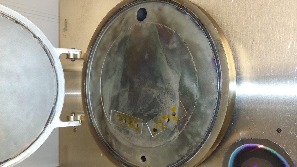
SiN chips (TEMs and Sepcons) taped into the PVD-75 platen, just before depositions.

SiN with 4.3 nm Ti and 12.1 nm Ag:

SiN taped to slides in ALD:
SiN with 4.3 nm Ti and 12.1 nm Ag, coated in 10 nm Al2O3:
As shown in the pictures, I used kapton tape on the chips. Since we’ve fixed the ALD gusting problem this was not for the protection of the chips, but instead a crude attempt at masking the bare silver from the alumina so that later I can attach leads to the chip. When I removed the tape, it seemed to have done a good job of keeping the Al2O3 off the silver without taking the silver with it when it was removed:


Next, I used silver epoxy to attach copper leads to these bare areas.

I also made this little monster as well:


I measured the resistance across all four points – 6 unique measurements in all:

I searched for a long time for hard numbers on the conductivity of silver films in our thickness range, and the closest I got was this paper (resistance of silver on glass), which found that 8 nm Ag on glass had a conductivity of 54  /square. Apparently any square of a given thin film has the same resistance across the diagonal, regardless of how long that diagonal is, which is mind blowing in a minor sort of way. Since I measured resistances of 25-42 for a 12 nm thick film this seems reasonable.
I think the takeaway here is that I don’t need to shield with kapton tape during the Al2O3 depositions, although I’m on shaky ground here and perhaps someone with a better background in electronics can comment.
The next steps all involve sticking the one-lead chips into my zetapotential setup. I made some 10 mM KCl (1 mM phosphate buffer) standard electrolyte solution, and I need to find the resistance between the chip’s lead and one of the Ag/AgCl electrodes within the setup while the whole thing is immersed in electrolyte. I also have some silver chips without Al2O3, and I plan to attach a lead to one of them and see the resistance between that and the Ag/AgCl electrode. With luck, the alumina will insulate charge from escaping into the solution.
After that, I will pump the electrolyte through the chip and see if I can get different zetapotentials if I vary the voltage applied to the copper lead. Once I’ve demonstrated I can dynamically change the zetapotential, my nanofluidic transistor won’t be far off:
