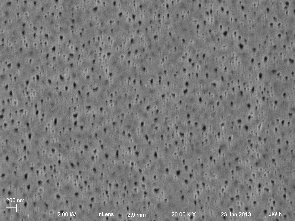
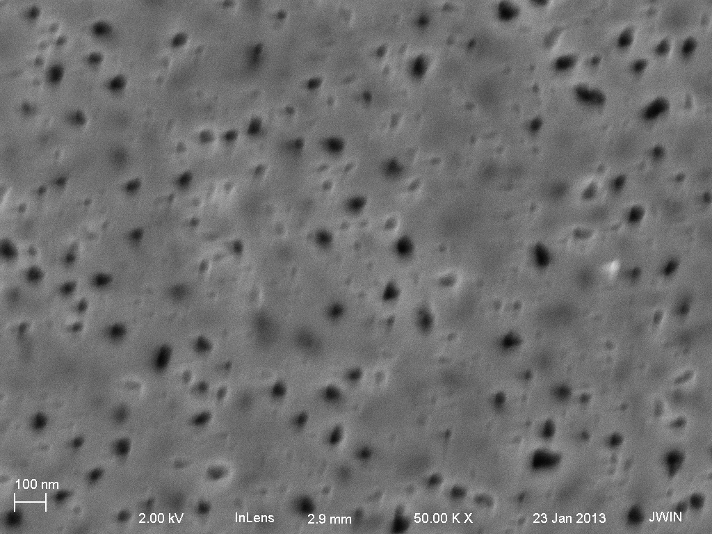
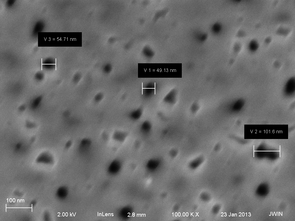
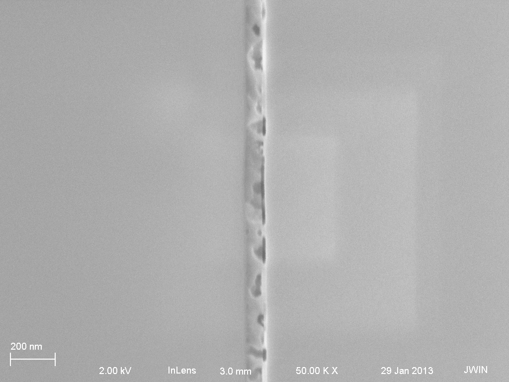
Pores in 60 nm pnc-Si
We deposited a 20/60/20 nm OSO stack for an ellipsometry test. We decided to try annealing the un-patterned wafer in the RTP at 1050 C with no susceptor with a 100 C/s ramp for 60 s.
The attached SEM images show pores forming. With these encouraging results, we are considering depositing 40, 50 and 60 nm thick a-Si on patterned wafers to re-investigate pore formation taking advantage of all of the latest advances in processing.