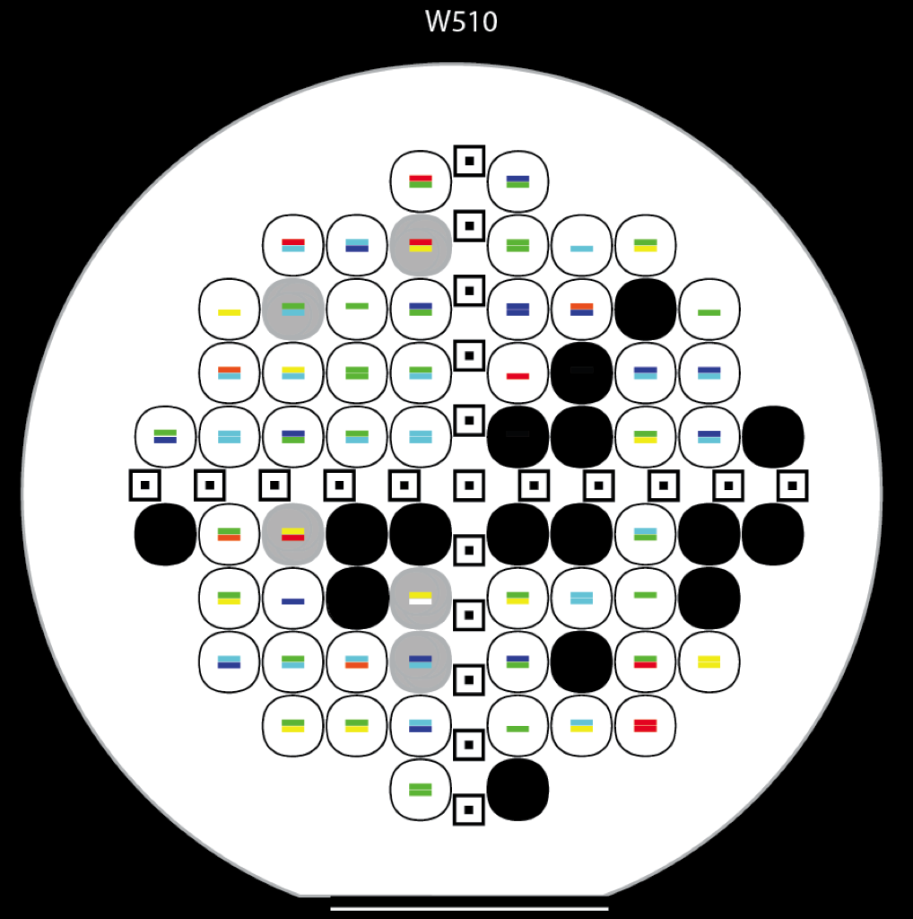
Pinhole Study: W510
To improve our knowledge of pinhole formation I have started counting pinholes on W510, W512, and W513. I also am playing close attention to areas surrounding the samples that have been completely etched, to see if this correlates to pinhole number. A schematic of W510 with number of pinholes is shown below. I would like to improve the presentation of this data, so feel free to make suggestions.

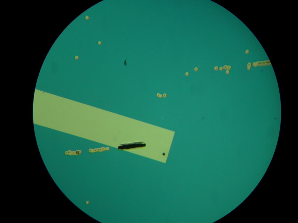
For intact wafers I plan on placing a black “X” on the outside of each sample to indicate complete etching. I also took images of some interesting things I saw.
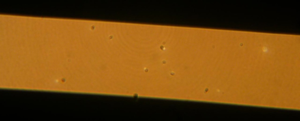
Impurities/contamination next to pinholes (-3,4)
Trail of pinholes (contamination?) (-4,-3)