TEM images of Ti+Au coated membranes (Wfr#313)
The coating was done last week at RIT (it was postponed from two weeks ago because of the failure of the e-beam crystal sensor). I deposited 10nm Ti and 15nm Au, without vacuum breaking. All the samples are from wafer #313.
TEM images were taken yesterday with the help of Karen. (Her machine is really much better than Brian’s old one! 🙂 We got some good images. The surface morphology is still rough but we have open pores after coating! The quality is comparable to that of a single Ti layer coating.
(I tried to paste TEM images of wafer#313 from the database for comparison, but I couldn’t find them at this time.)
I am going to test permselectivity next week with these samples (since now we are sure that our coated membranes are conductive, not very good conductors though).
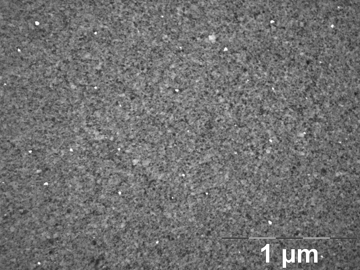
Fig.1) 10nmTi+15nmAu (30K)
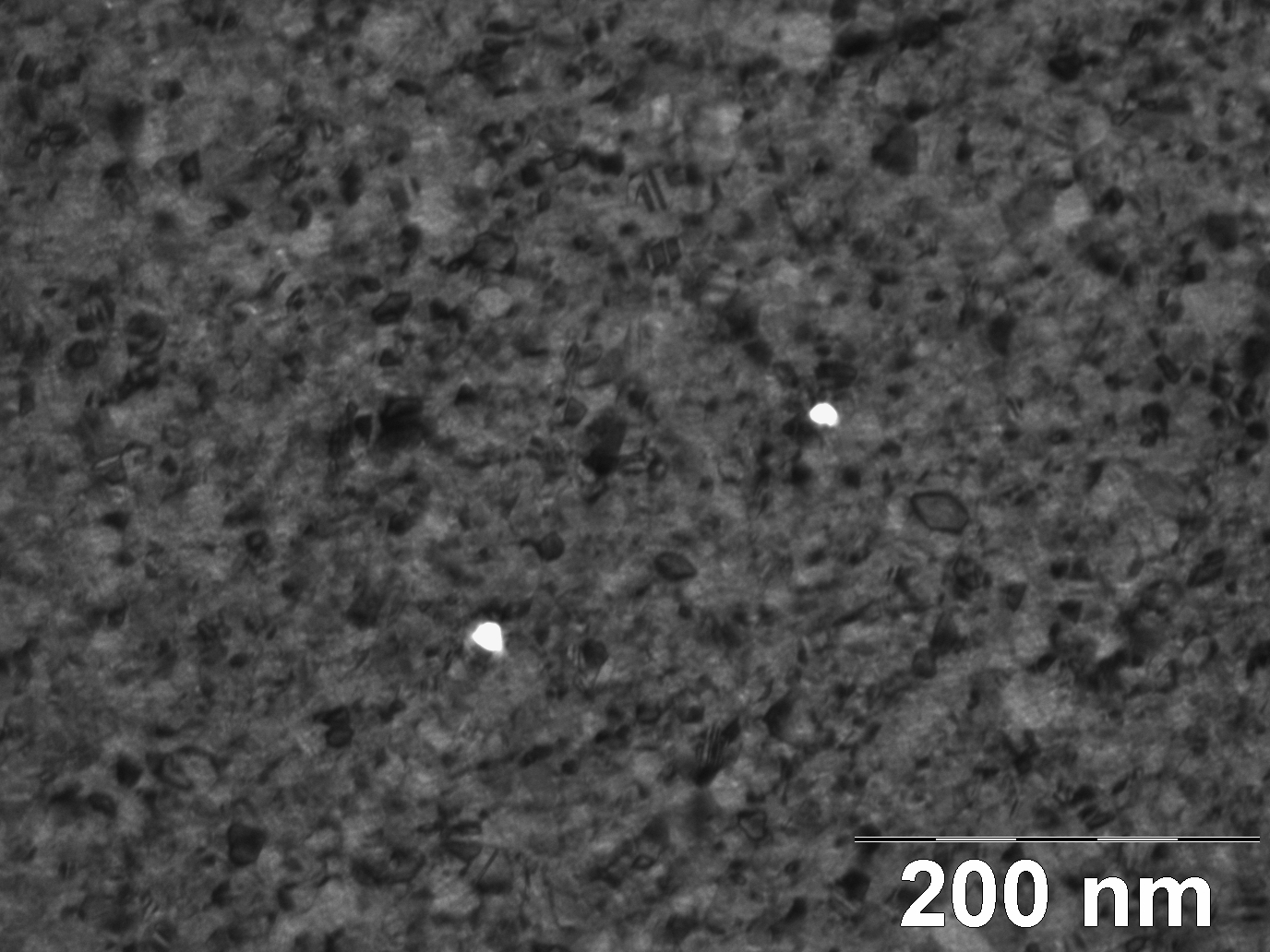
Fig.2) 10nmTi+15nmAu (150K), the two pores are abt 20nm
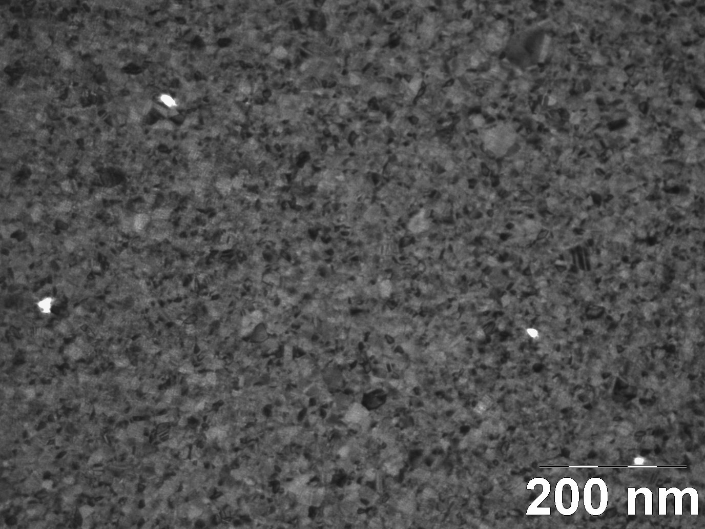
Fig.3) 10nmTi+15nmAu (150K), the pores are abt 15nm