This is probably not of general interest, but for the sake of full disclosure, I have spent considerable time working with our wafer supplier (Virginia Seiconductor) to resolve some issues regarding the surface quality of their wafers. It would have been much more productive to simply switch suppliers, but unfortunately, they are the only place I could find that will make a custom thickness wafer with tight thickness tolerances. Since this is very important for producing membranes with similar geometry run-to-run, I decided to work with them.
Early roughnes problems have been resolved, however a lingering problem is a high concentration of 3-4 nm particles on the surface of their new wafers. They have introduced a new megasonic cleaning process to remove these features, but they are still there, as shown in this new AFM scan:
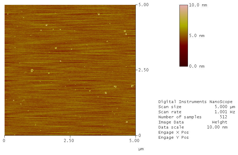
We have shown that they are removed by our oxidation and subsequent stripping/cleaning production process (before membrane deposition), so I do not believe they are an issue for us. However, I will continue to work with the supplier to improve their process, since it would best best to eliminate this issue.