Electron Beam Lithography Microchannel Fabrication
This post is a continuation of project found in Fabricating 0.5 um Channels in Microscope Slides for Staph Invasion Assays.
Just to review, after the development of μSiM-CA (Canalicular Array; see Masters et al., Nanomedicine: Nanotechnology, Biology, and Medicine 2019), Jim wanted to develop a platform to answer some more biophysics focused questions. In order to facilitate these studies, the platform would ideally be configured to allow for live imaging of staph invasion into sub-micron spaces.
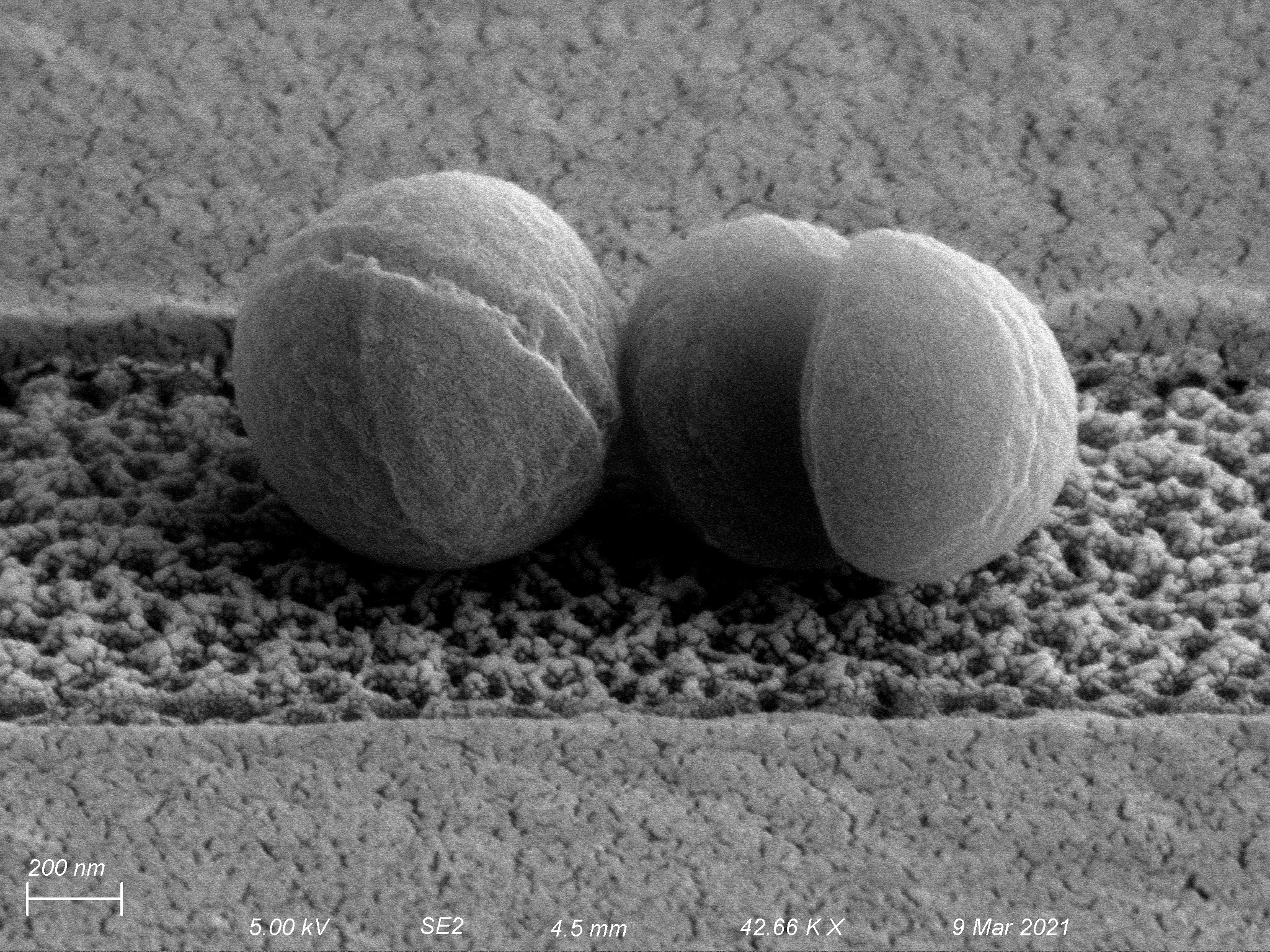
We are trying to create micro and nanochannels for the confinement of bacteria. It’s thought that these bacteria can squeeze into small spaces (~0.5 micron), less than the size of the bacteria itself (~1 micron diameter), and avoid antibiotics in the body. Our previous attempts made some progress with the laser writer, making channels that etched into glass. Ultimately, these were too thin, too wide, and not porous. The bacteria did not enter the channels, and we could not study their behavior there.

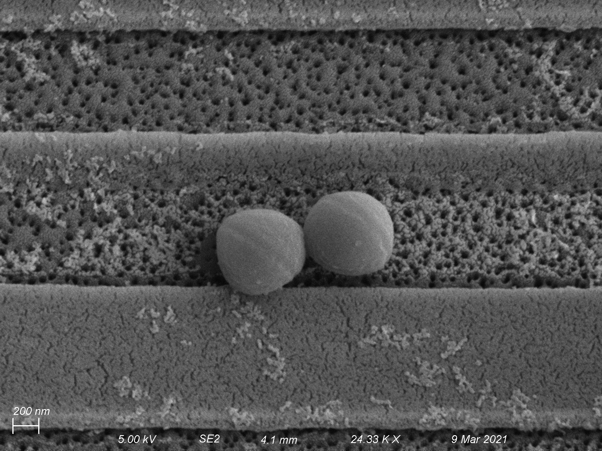
To better capture the behavior of the bacteria, we would like to confine the bugs in 500 nm wide, 500 nm tall channels, while still having permeability. Channels fabricated on top of NPN would be ideal here, as the material would permit gas and nutrient exchange even in these small spaces. However, our previous methods for manufacture using the laser writer were not good getting down to these small geometries. To better create these very long, very narrow channels, we used electron beam lithography to directly fabricate the channels in PMMA, a resist that is biocompatible when fully crystallized.
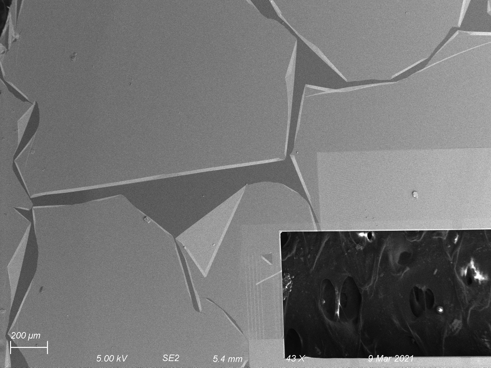
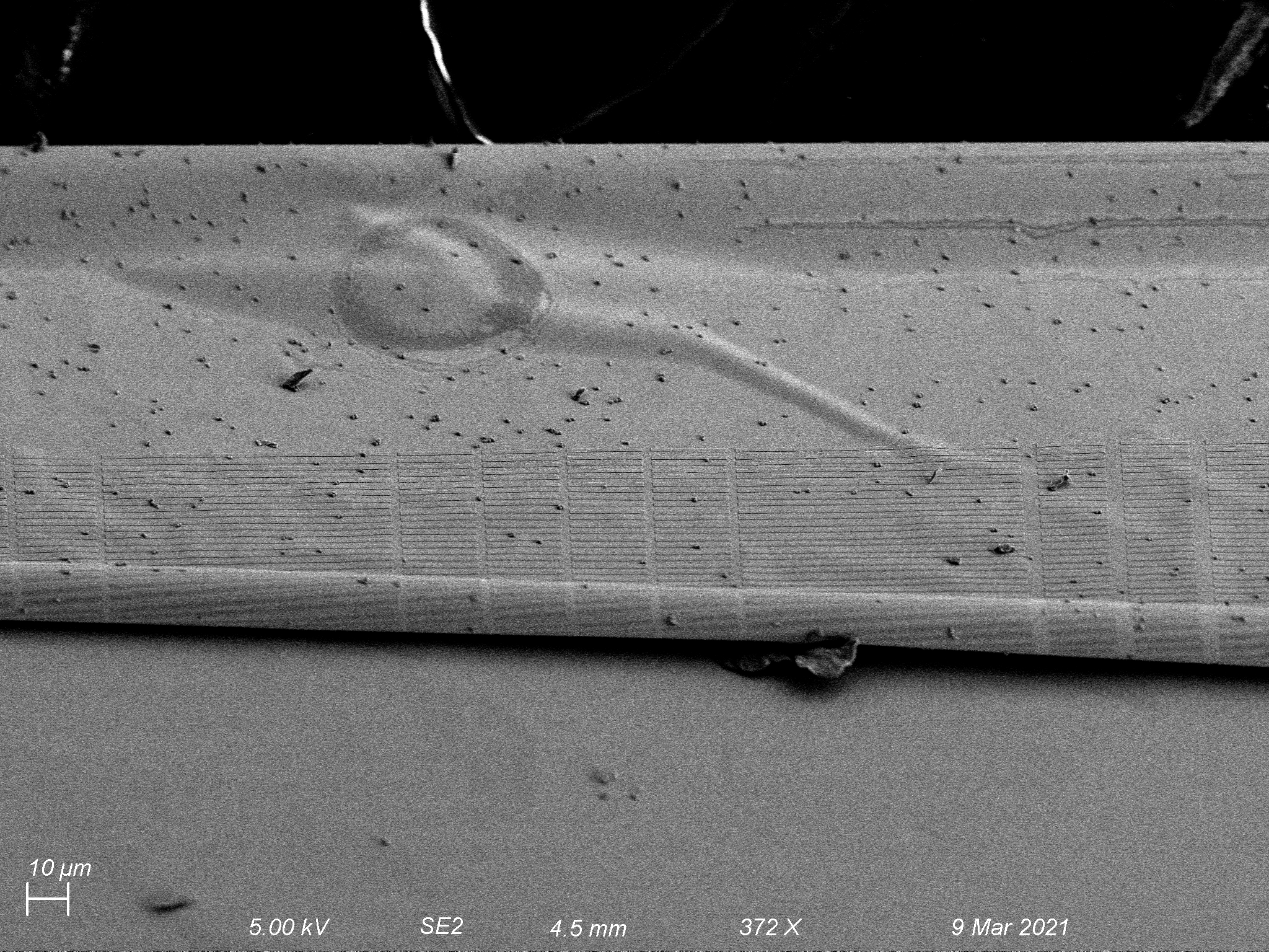
After a few development runs, we designed channels that were 500 microns long and connected by pads at the end of each grouping (A). While fabricating, the electron beam deflects to stencil the desired geometry, to prevent energy of the beam going into places where we are not patterning. However, in practice, this is not perfect, and there is some residual energy over the area of the window where we are writing (B) and (C). This leads to overexposure and wider features than we originally desired, but it turns out that the raster pattern led to small sub-micron channel features that were ideal for what we were trying to accomplish!
The settings that led to the most successful fabrication conditions were:
Coating
- Use a bit of carbon tape on a glass coverslip to affix NPN chip in center of coverslip
- Dispense URnano’s PMMA A3 resist on chip so that it covers the entire surface and immediately begin spinning
- Spin for 3000 RPM for 45 seconds
- Remove chip with tweezers and place on 180C hotplate for 60 seconds
- Setting in URnano is 250C on the hotplate, then place on on Al block in center of hotplate.
- This is critical to smoothing out perturbations from spinning at lower speeds.
- Cool chip on Al plate
- Datasheet Reference: https://www.lsu.edu/camd/files/MicroChemPMMASeries.pdf
- The resist is a little thicker than indicated, due to the small chip area and relatively large amount of resist dispensed. Edge bead inhibition.
Lithography
- Dose range between 0.01-0.05 uC/cm^2. The channel features require lower doses, and the pad features require higher doses
- 1 uS dwell time
- 50×50 nm pixel spacing
- 30 um aperture. Larger apertures have higher currents and shorter write times, but this exacerbates the overexposure raster problem.
- 30 kV accelerating voltage
- The magnification to write the whole membrane area is around 50x; higher fidelity patterns will be easier to write if the field of view is smaller.
- Manual alignment to window calculated by stage move; mark a fiducial near the edge of the chip to position the beam without accidentally exposing the resist.
- Overall, this pattern took between 30-60 minutes to write.
Development
- Immerse chip and agitate for 40 seconds in 3:1 IPA to MIBK developer solution
- Rinse chip and agitate for 40 seconds in IPA
- Immediately use compressed air to blow dry the surface of the chip
Characterization
- Coat with 5 nm Au to enhance contrast (100 mTorr, 50 sec Ar plasma in Denton Sputterer).
If I were to make another set of devices, I would spin at 2500 RPM, write around 0.01 uC/cm^2, with a 20 um aperture. It might take a few hours to complete the pattern; It’s a very sensitive process, and we have learned how better to write on the membrane with each development run.
We intend to seed some on these devices by direct centrifugation (~200g) or using flow to site cells on the NPN by suction through the membrane in a uSim format.
UPDATE 03/10/2021
Centrifugation didn’t work so well, but Alec was able to draw down some bacteria onto a 4krpm device. Ethanol was used for fixation, but it attacked and lifted off the resist patterned channels. In the future, we should fix, then dessicate immediately. The membrane cracked as I lifted it out of the ethanol, but the fragments wrapped around to the trench of the chip, and we were able to see the relative thickness of the bugs in the submicron channels!