The effects of driving pressure on sieving behavior in SiN Sepcons
We’ve been wondering for some time just how the thinness of our membrane will affect the concentration polarization behavior of solutes. Because solutes with sieving coefficients less than 1 are (by definition) moving slower than the solvent around them, in the area before the membrane their concentration increases. In the case of proteins, this so-called concentration polarization leads to cross linking and a faster rate of cake layer formation, resulting in lower hydraulic permeabilities and lower sieving coefficients. To prevent this, cross-flow filtration, where the solute is flowed parallel to the surface of the membrane, is used. In applications where dead-end filtration is unavoidable (such as Sepcon-format SiN chips) flows are kept low so that diffusion back into bulk solution can partially counteract the concentration polarization. I’m hoping to demonstrate that SiN can potentially benefit doubly from slow flow rates in dead end filtration. This is because not only can solutes diffuse away from the highly concentrated polarized layer back to bulk, but the thinness of the membrane means they can also diffuse through the membrane.
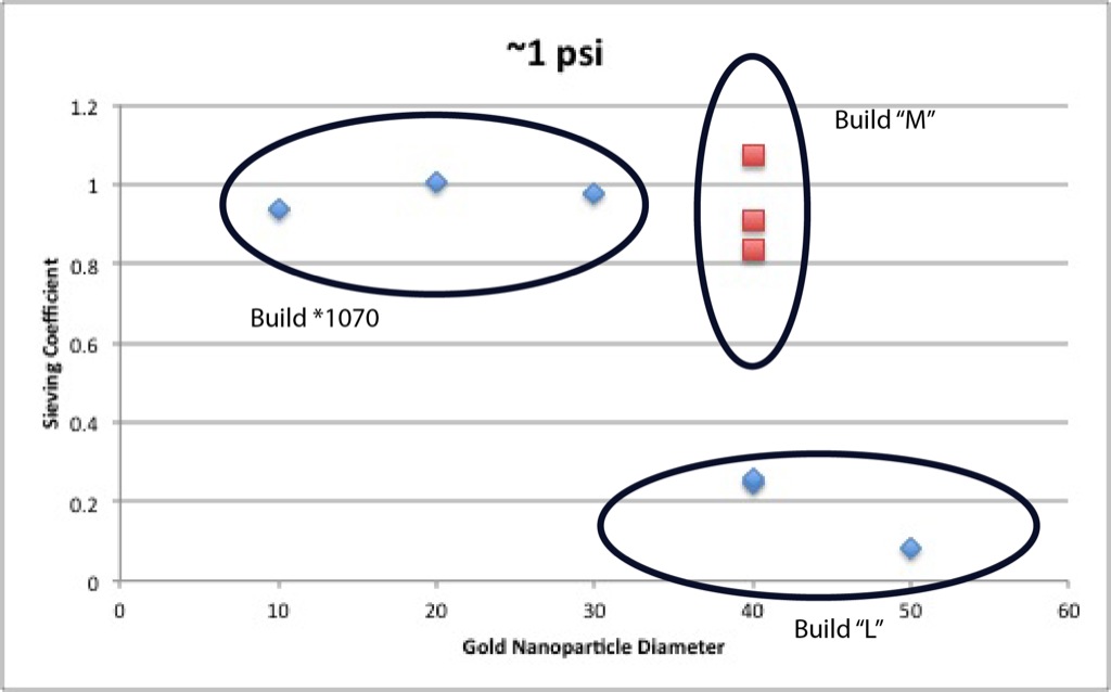
Methods: I’ve been on an assembly kick lately and these experiments represent three separate Sepcon builds, labelled “*1070”, “L”, and “M”. All chips were broken out of wafer 1070 (<40 nm> & 20% porosity) and their nitrogen permeance at 5 psi was measured using the unitless and mysterious green flowmeter. All gold was prepared the day of the experiments from BBI stock solutions kept in the fridge. Barnstead water that had been passed through a 0.2 micron Pall aerodisc filter was used to to make 4:1 dilutions (3 parts water added to 1 part gold stock). Care was taken that 40 and 50 nm gold particles were well vortexed before the dilutions were made, and well mixed before loading. Sepcons were loaded with 300 uL of sample and fitted onto our custom teflon pressure fitting. Nitrogen pressure at the given psi was applied until ~200uL of sample had been collected into the outer baskets. Outer baskets were weighed before and after sample collection to get volume passed, and the time of collection was noted for hydraulic permeability calculations. Standard curves were made using dilutions of the 4:1 solution. Absorbance was measured using the very chipped cuvette in the Tecan at the absorbance peak of the 4:1 dilution, which for 10, 20, 30, and 40 nm gold was 525 nm, and for 50 nm gold was 530 nm. Chips from my “*1070” assembly were used for the 10, 20, and 30 nm gold data. “L” chips were used for the first set of data on 4o and 50 nm gold, and “M” chips were used for the dedicated 40 nm gold data.
You can find my raw data, including standard curves and hard absorbance values, in this excel spreadsheet.
Data:


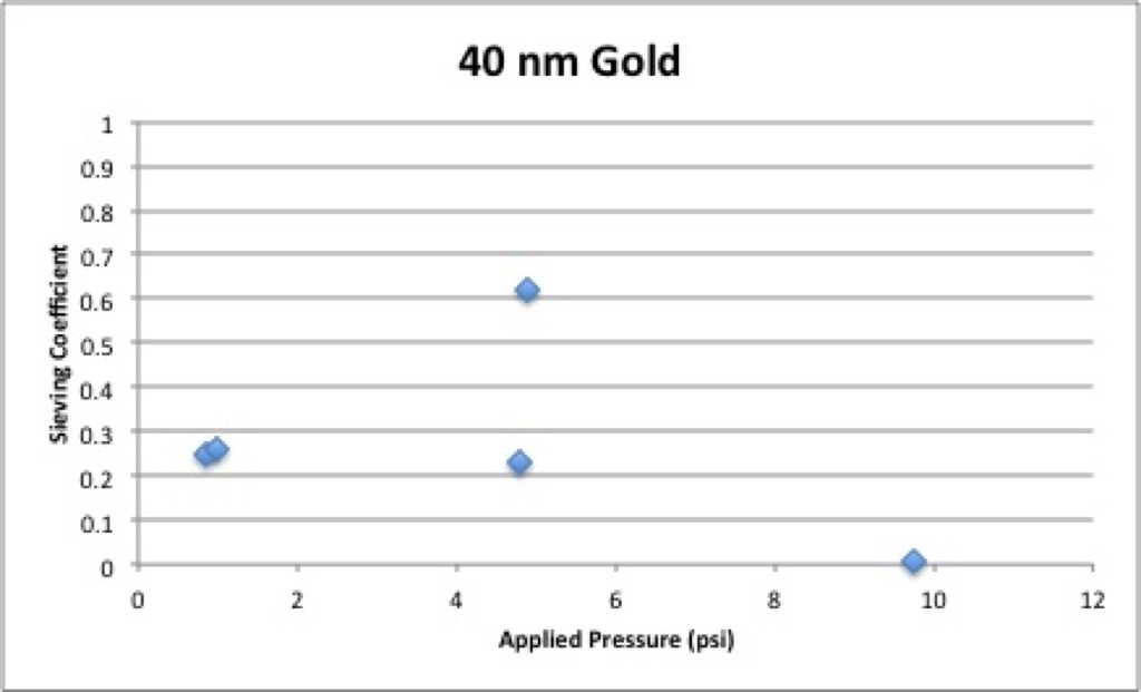

The story that I saw from this first set of data made a lot of sense to me. Everything smaller than and including 30 nm diameter gold goes through the pores unimpeded, with sieving coefficients approaching 1. At 40 nm and above, gold flow is impeded. Since wafer 1070 has an average pore diameter of ~ 40 nm, this made sense. If pressure had anything to do with the sieving coefficient, I couldn’t yet tell, but these were preliminary experiments designed to show me which particle size I should focus on. My next task was to repeat the 40 nm gold experiments. Those results were more frustrating:
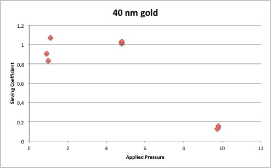
Combining the two sets of data for 40 nm gold gives the following, where here (and in all subsequent graphs) blue represents the first round of data and red the dedicated 40 nm gold data:
Although it’s nice that there is clearly some sieving coefficient dependence on the pressure at high enough (>5 psi) pressures, the lower pressure data is all over the place.
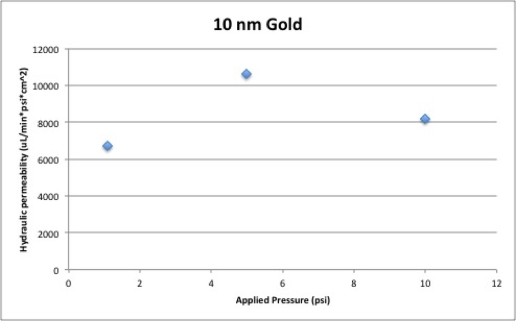
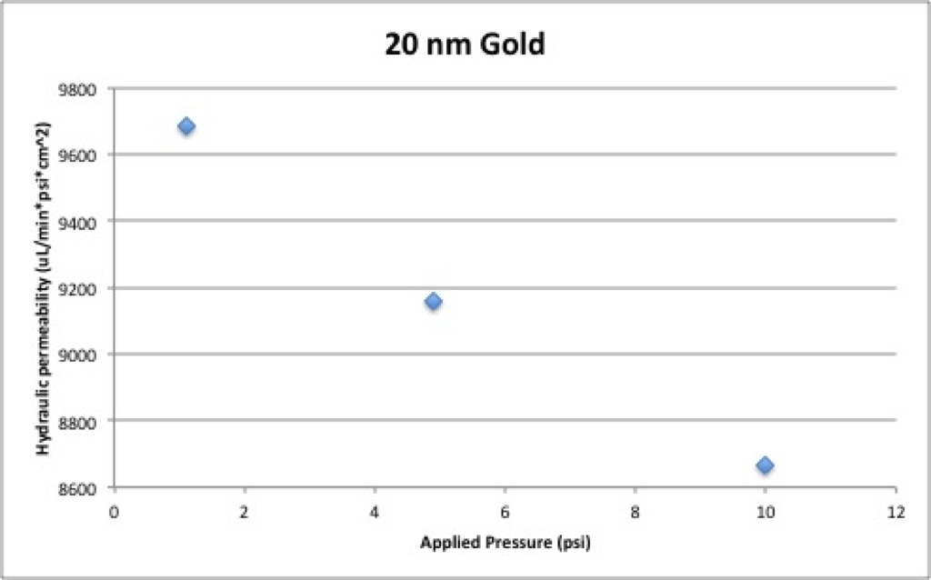
For comparison, I’ve also included the pressure vs. permeability graphs for the five gold sizes below.


And also gold size vs. sieving behavior for the different approximate pressures:


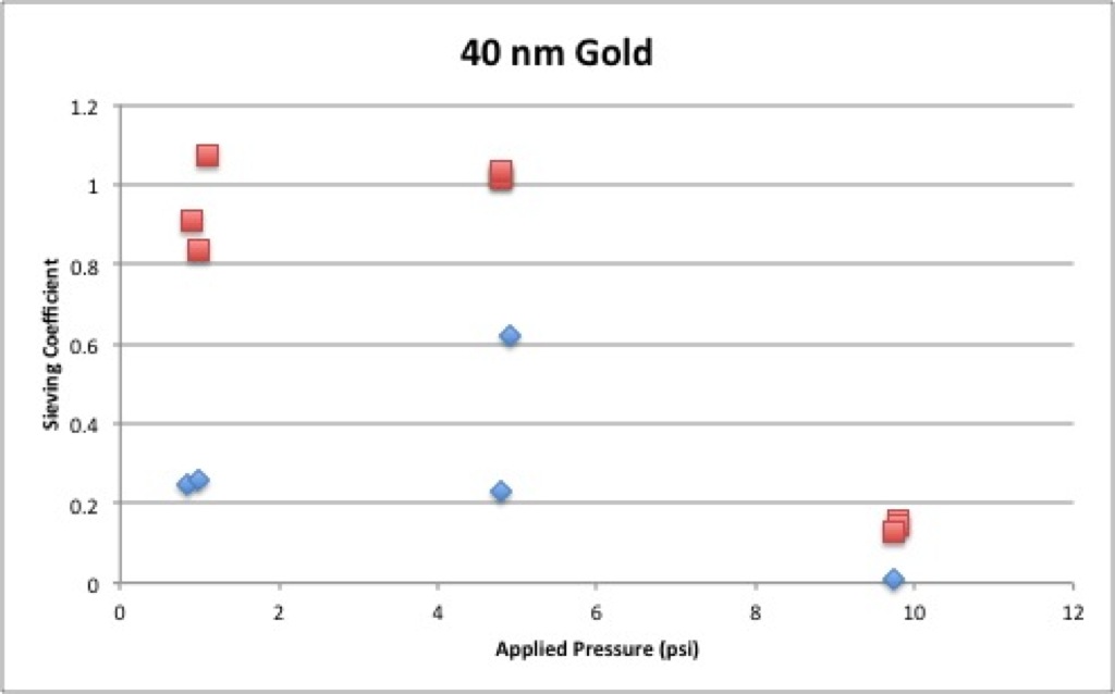
It’s also worth examining the two 40 nm gold plots above (pressure vs. sieving coefficient and pressure vs. hydraulic permeability) next to each other:
What’s odd here is that at 5 psi I have two clear outliers, but both outliers only outlie on one of the two graphs. I’m not sure what, if anything, to take from that.
The troubling conclusion I’ve come to is that within an assembly batch or testing batch I get fairly consistant performance, but across different assembly or testing batches there is significant variation:
When I measured permeance using the green and mysterious flowmeter, I measured average flows of 4.2 units for build *1070, 1.6 units for “L”, and 2.1 units for “M” (this data is included in my excel spreadsheet linked above).
I assembled all of these chips and to my knowledge I didn’t change anything in my process between them. I double checked the thickness of the gaskets. Some other possible sources of variation in performance that Josh and I have discussed include the humidity of the lab, static charge buildup during assembly (especially when the protective gasket sheets are peeled back from the gaskets), and the age of the gaskets (repeated use of a set of gaskets can make them dusty). I had made a new dilution of 40 nm gold between the M and L data sets but used the standard curve generated from L for both, and so I went back and measured the diluted gold for the M data set. The absorbance was 10% higher in M, but I attribute that to evaporation, and even if they were different 10% wouldn’t explain the full difference.
After discussions with Josh, I think I am seeing the variability of the pore distributions across the wafer. The chips may perform similarly within “builds” because they come from a similar spot on the wafer. Ideally we would like to be able to use all the chips on a wafer interchangeably, and use a fresh chip for each data point, as I have done in this post. But at least for the time being it may be better to use the same chip for multiple data points.