Nanoporous Nitride Membranes: 400-µm wide channels, a pictorial survey
Images of the nanoporous nitride wafer. The same wafer that Josh declared as having 30% porosity with an average pore size of 80 nm (or something similar). Josh put images and such on basecamp for those who have access. These numbers are for a TEM grid from near the outside edge of the wafer, where all the TEM bits are located. This wafer was delivered with a reported yield of 6 out of 21. This is the first nanoporous nitride wafer with such large surface area.
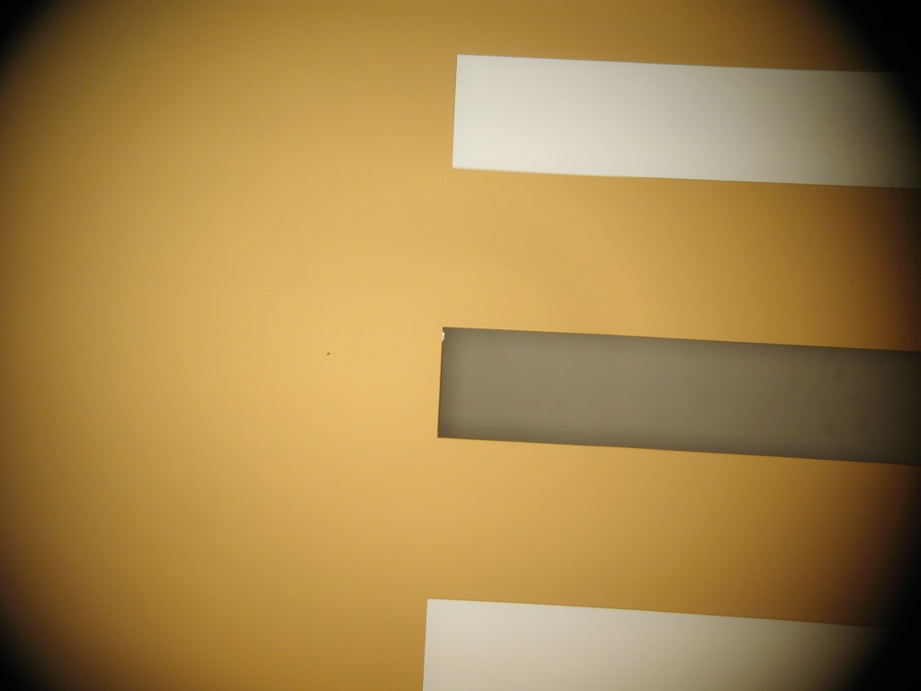
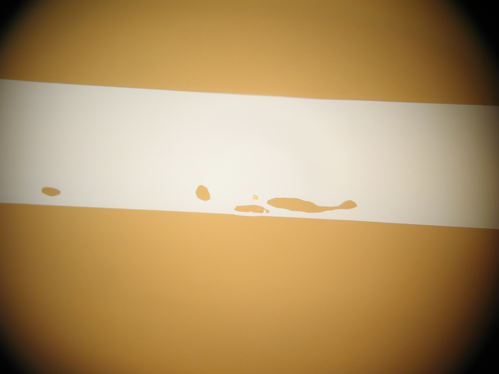
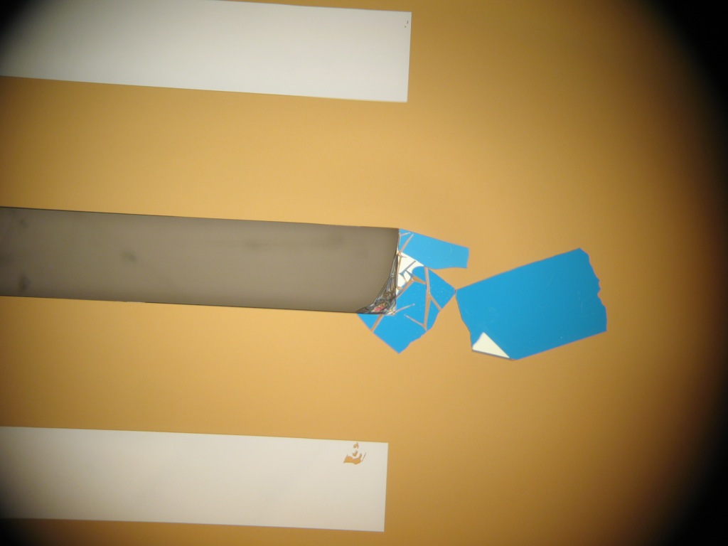
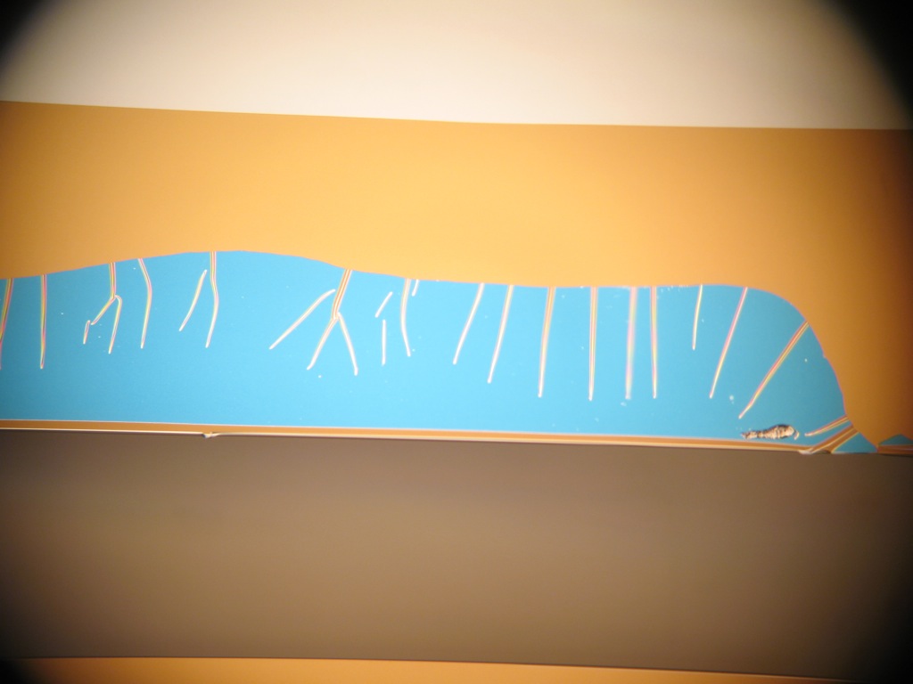
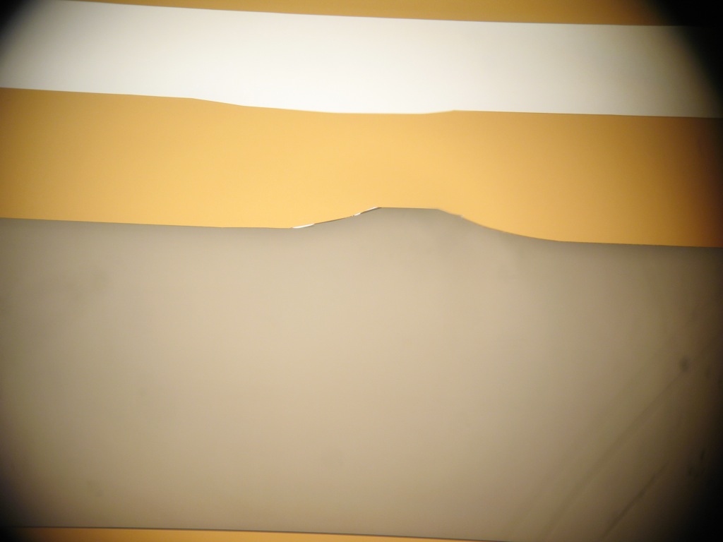
Clearly there is something going on with the formation of the windows as they can be very rectangular, but occasionally not. Some odd shaped membranes survived, those with the most significant deformities did not. In fact, the most massive destruction occurred on chips with these deformities.
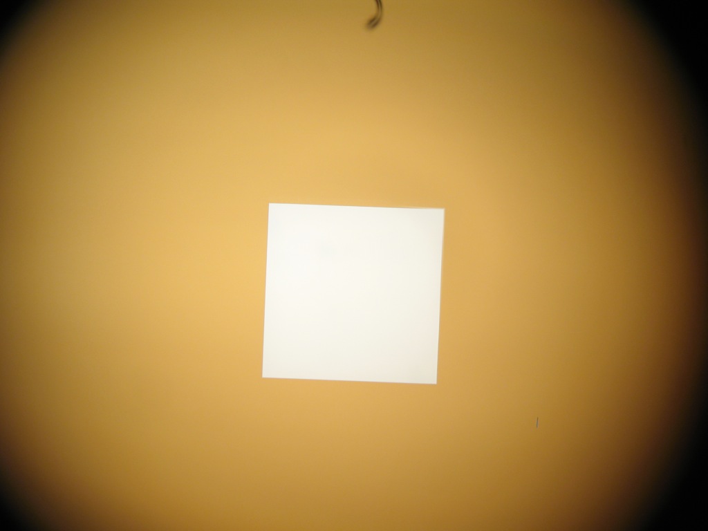
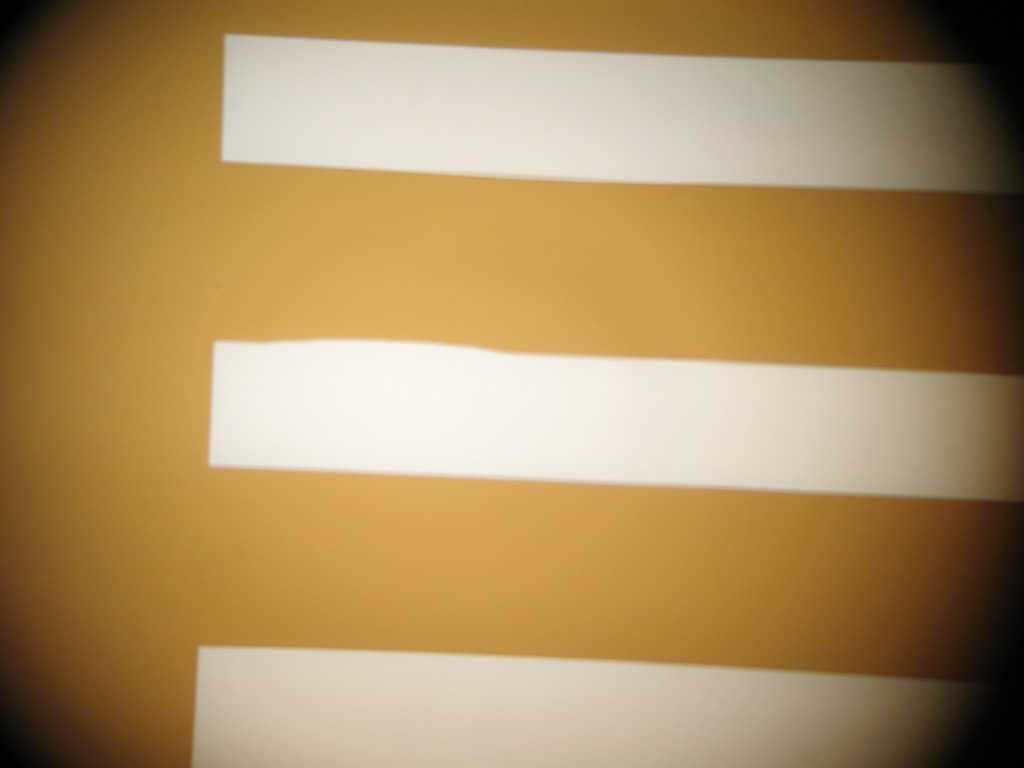
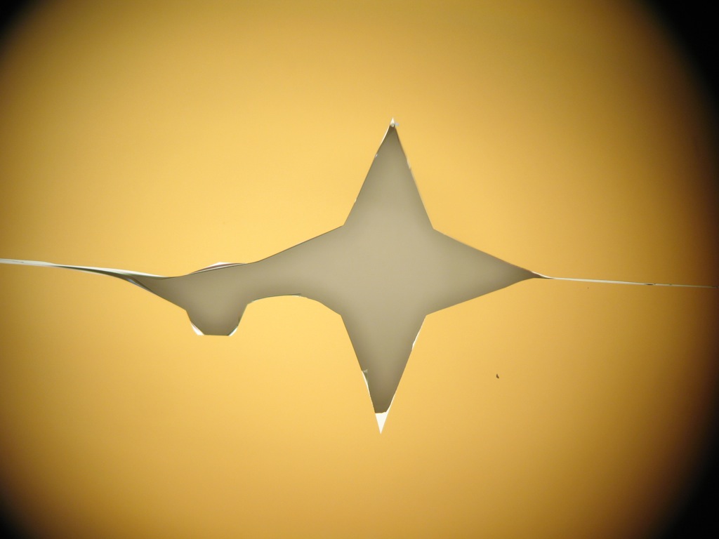
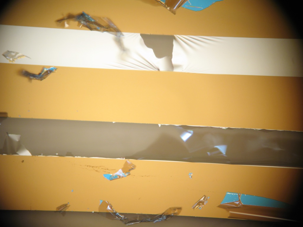
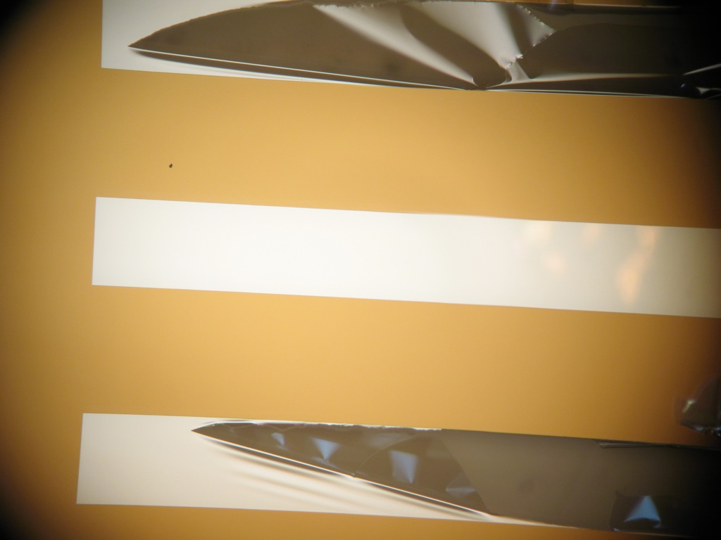
Most images are 5x, others are 10x. The first image is of a square to be used as a fluid via, the second is a TEM grid. The star shape, later on, is the intersection between four chips. The rest are channels, 0.4 mm by 15 mm.


These next three are 10x


Another 10x


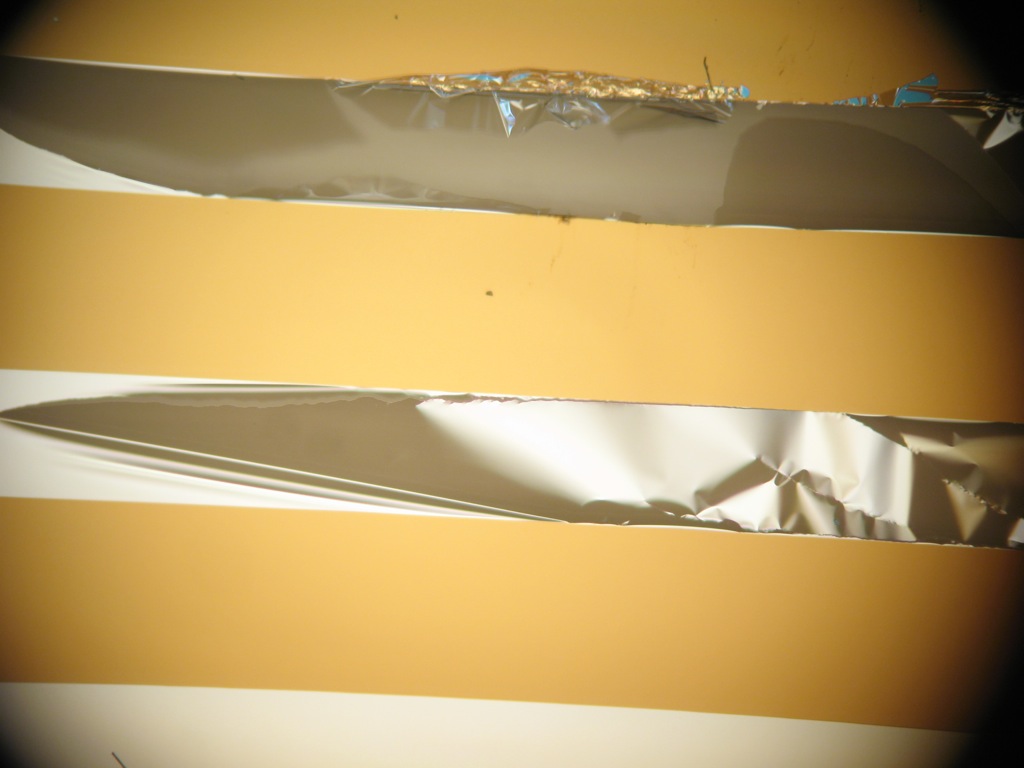
These are obviously the bad chips, but the overall yield was 8/21, right? Are the good chips holding up to device assembly?
I assembled a 2-chip device today using gasket material. It held up well to the fabrication process with one exception. The backside chamber roof needs to be thicker so it doesn’t sag and contact the membranes. This may seem obvious, but it is hard in practice to keep this from happening while removing the gasket backing material.
I have a mask on the way for creating the molds I need to make PDMS-based devices so this won’t be an issue.
I did break two chips: the first was a complete loss of membrane in one channel during chip pop-out. the other suffered a small tear of one membrane while soaking it in ethyl alcohol.
In short, the membranes which make it off the wafer and out of the rinse faired well.