Negative Data for Nanofluidic Transistors, Dielectic ‘Flowers’, and an Interesting Gold Filtering Behavior
I’ve been trying for a year now to make a nanofluidic transistor – a nanomembrane with a thin layer of metal coated in dielectric that allows for the dynamic modulation of the sieving characteristics of the chip.
Beginning with the last 14 chips from wafer #1081, I coated them in ~3 nm of Ti and ~12 nm of Ag, then used the ALD to deposit 10 nm of Alumina. The ALD has had a bunch of problems lately, and in particular the vacuum in the chamber is too weak for the standard low temperature alumina recipe that Ryan Beams developed a few years ago. With Alex’s help I tweaked the recipe, but the vacuum has become worse over the past few weeks and I was only able to get through the process by increasing the overpressure automatic stopping threshold from 250 torr to 500 torr. Once that was done, the machine did seem to do a nice job.
I measured the IV sweeps for two different chips using the procedure outlined in an earlier post. Both chips demonstrated the electrical characteristics I’ve come to expect from intact chips – that is, between -2 V and 2 V, the current varies less than 0.1 uA, but after popping the chip by taking the voltage up to 15 V, the current varied by around 0.8 uA. After removing both of these chips from the zeta/IV chamber, I imaged them in the microscope:
Chip 1: Notice the odd ‘flowers’

Chip 2. The file linked is a movie of the chip drying. I include it so that it’s clear that these ‘flowers’ aren’t salt crystals.
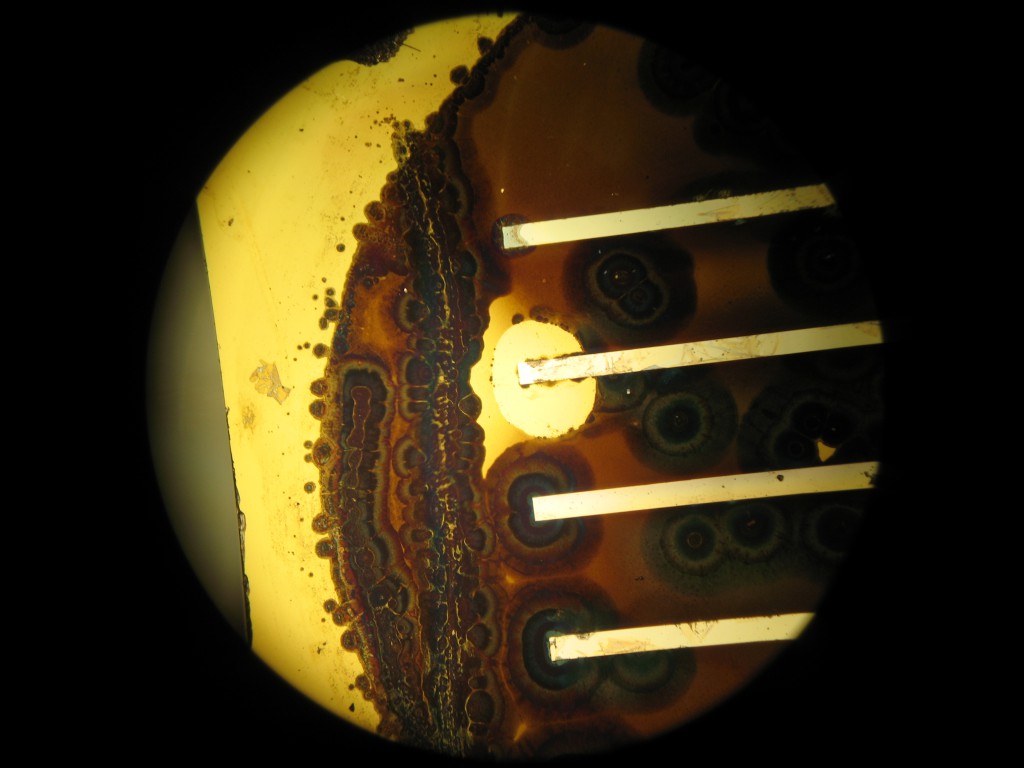
My hunch is that these ‘flowers’ are the places where the dielectric actually popped and allowed current to flow. I’m not quite sure how to verify that, or even if it would be useful to verify that, but here are the images nonetheless.

(Also, what’s with that little triangle? Is it the missing piece from the triangle-shaped hole above? Weird.)
Vertical slash in the next two images is a tweezer scratch:

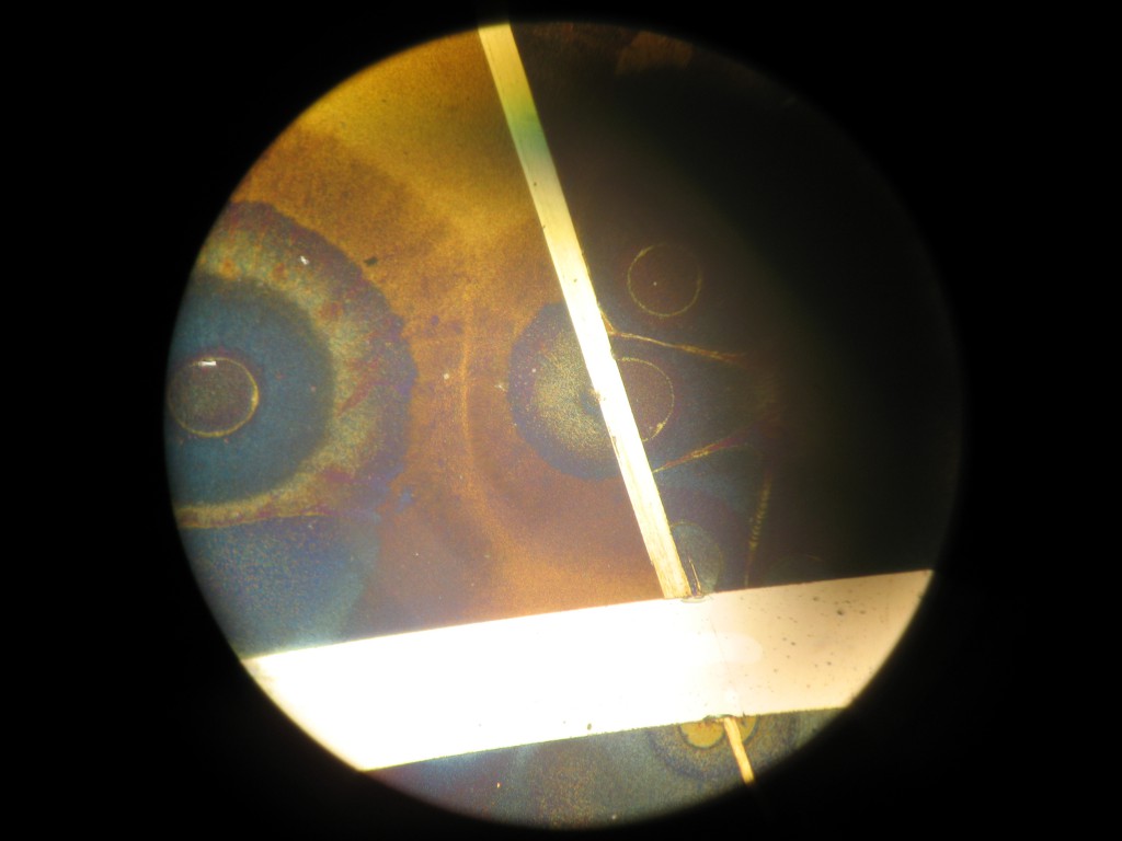
Image of a broken chip I put in the zeta setup for about five minutes. No flowers.
So it seemed like the chips were 1) conductive and 2) insulated by the dielectric. Hopeful, then, that I could demonstrate some changing sieving behavior, I threw them into a modified pressure setup:
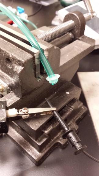

I couldn’t find the polycarbonate fitting we’ve used to attach the nitrogen to the sepcons – there’s one at the Simpore office, and a broken one on the desk, but we had a third one that is as of now missing. Instead, I twisted off the cap of one of the 1.5 mL conicals we use for sepcons, drilled a hole through it, stuck a length of green tubing through it, and coated the whole thing in vacuum grease. It worked so much better than it should have – the seal seemed perfect.
Based on some experiments I had run in the hours before I left for BMES, I started with 200 nm of 5 nm gold nanoparticles (mixed 1:1 with barnstead water). They flew through – roughly 100 uL in 12 minutes. So washed the chip thoroughly and switched to 40 nm. They flew through too. 50 nm went right through, and now I was worried that the chip was broken or there was a leak in the seals or something odd, so I jumped to 80 nm, which was retained. Phew. Then I went to 60 nm, and nothing went through. So I went to 50 nm, and nothing went through. This confusing set of experiments is illustrated below. The progression is indicated with arrows. Some of the experiments were conducted with small applied voltages, and all of these were done on the same chip:
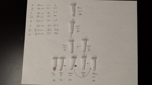
(ignore the numbers in the upper left corner)
What’s neat is that the gold cutoff starts at greater than 50 nm, but after retaining 80 nm gold in a separation, the cutoff shifts downwards to less than 50 nm. Hydraulic permeability fell too, although probably by only 60% over the course of all the experiments. So perhaps 80 nm gold gets physically stuck in the largest pores?
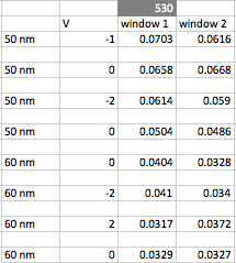
Next, I used another chip and started with 60 nm gold. I applied -1V, collected ~40 uL of filtrate, switched to 0 V (collected ~40 uL), then -2 V, then 0V. On visual inspection, lots of gold passed in all of the separations but no more or less in any of the voltage configurations, which i confirmed with the TECAN and the nanoquant plate (all absorbance measurements were within noise of each other). So I switched to 60 nm gold (but using the same chip as the 50 nm separations). Here the sequence was 0V, -2 V, +2 V, 0 V. Here no gold passed in any of them, again confirmed with TECAN. I was technically monitoring the current while the voltage was applied to the chips, but I wasn’t watching the readout closely. It seemed like all applied voltages had currents low enough to be noise, except +2 V, which was noticeably higher than the others (~50 uA I think). Raw data below – absorbance at 530 nm on two windows for each data point. It’s not worth making up standard curves for these. No buffer signal is subtracted.
Conclusions:
It’s a terrible bummer that the separation behavior didn’t change with applied voltage. It’s possible that we’re not close enough to the cutoff to see the subtle difference -1 V or -2 V would have on the surface charge. Next I might try increasing both the thickness of the alumina coating and the applied voltages. Regardless, we need to wait for more large-pore chips from Simpore, which won’t get here until after break.
There’s something odd going on with the depositions of silver and alumina. I found that the same process (3 nm Ti, 12 nm Ag, 10 nm Al2O3) on <40 nm> pore size chips resulted in membranes that were totally gas impermeable, but doing the same thing to <70 nm> pore size chips resulted in pores big enough to pass 50 nm gold. I’m not sure what that means, if anything.
It’s worth keeping in the backs of our minds that we can change the separation characteristics of the membrane by doing separations with larger-size gold nanoparticles.