Film Stress w/ SU-8
SU-8 3010 has been used to create a scaffold in the fabrication of the liftoff membranes. The supplier of the negative resist, MicroChem, rates it for a 13 moth shelf life. We were having difficulty achieving good liftoff with membranes in the second half of last year. The SU-8 had expired by several months, so we were becoming suspicious that it was the cause. We measured film stress of this by coating a ø6″ wafer and exposing the entire surface (i.e., no mask to create scaffold pattern). The stress was found to be 25.6 MPa (tensile). Measurement done on Tencor P2 Profilometer to obtain change in wafer curvature. Control measurements on a 3 blank wafers show the threshold of detectability to be about 0.1 MPa.
We obtained a new bottle of the SU-8 and found that the film stress of this is 13.9 MPa (tensile).
We also were able to measure the stress of a patterned film by measuring the wafer profile from the rear face. The grid pattern covers the inner ~130 mm of the wafer and creates a square pattern with 10 µm wide struts repeating on a 110 µm distance. This corresponds to about 20% area coverage. From a highly simplistic viewpoint one could guess that the measured stress should drop proportionally to the amount of coverage for the patterned film. The ourter annulus that is not exposed (1 cm wide, 15 cm outer diam.) accouts for 25% of the total wafer area. The SU-8 pattern covers 20% x 75% = 15% of the wafer area, so to a very rough estimation, we might expect to measure a film stress of 15% x 13.9 MPa = 2.1 MPa for the patterned film. When we measure the patterned film, we see a stress of ~0.2 MPa.
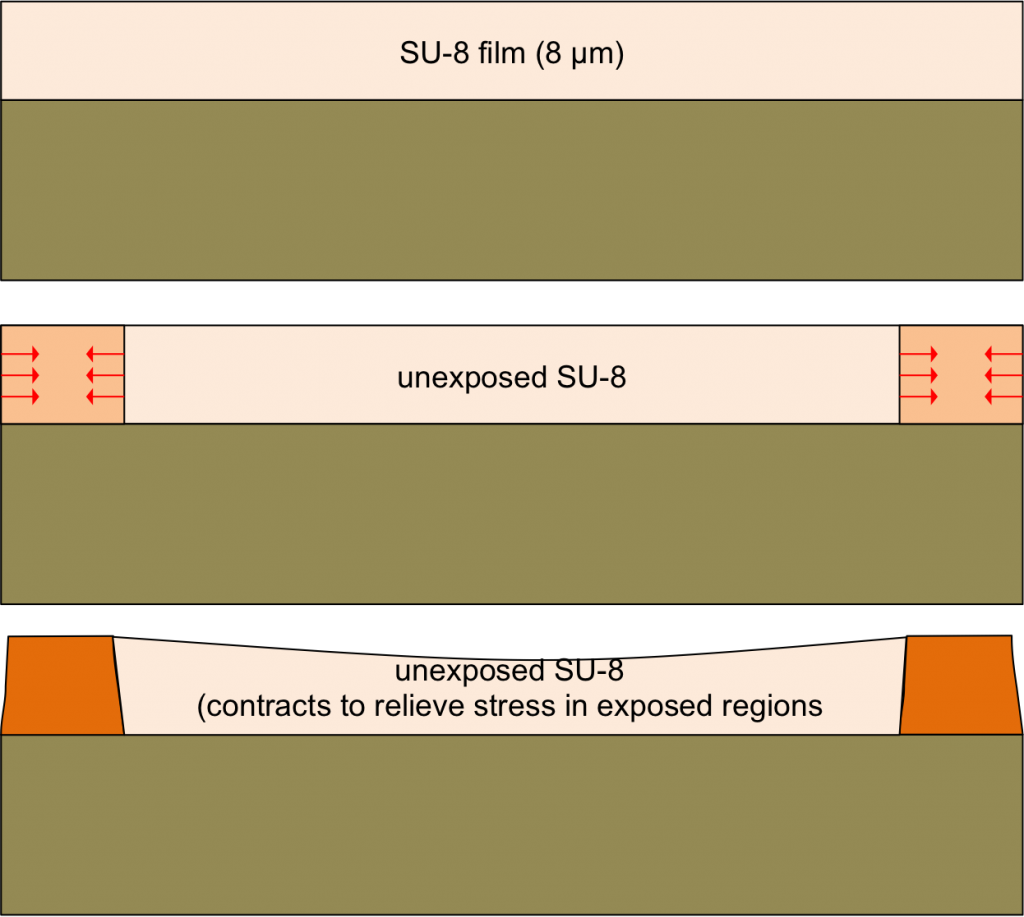
It could very well be that removing the outer annulus has a nonlinear impact on wafer curvature, but I am wondering if there could be some subtlety with residual stress in the SU-8 struts. If the stress results from the material shrinking as it cures and/or shrinkage as it cools from the cure temperature (mismatch in coef. of themal exp. from wafer), perhaps geometry of the struts (near-square cross section) enable relaxation away fr0m the bonded interface with the wafer. In the case of a continuous film, there is no opportunity for this. The figure below is a crude attempt at illustrating this with a cartoon schematic. On the left is the case for a continuous film. In the curing process the entire surface of the film experiences stress buildup and exerts this on the underlying wafer causing curvature. On the right, most of the area is not exposed and localized stress in the strut features can be relieved by pulling on the adjacent areas of unexposed SU-8, which remains in a liquid form. Note that these are not drawn to scale and the strains are highly exaggerated.

How much total wafer bow are you measuring in these experiments? With 8um of photoresist, I would guess that you could have +/-1um of thickness nonuniformity, which could be a problem for measuring very small curvatures. If you are measuring <10um of curvature, I would be less concerned. Are you able to measure the same coated wafer before and after exposure? This might normalize out this effect.
Assuming the measurements are beyond the noise of photoresist thickness nonuniformity, I think some contraction of the PR during cross-linking is perfectly reasonable. The stress is also quite small, which is also what I would expect for an organic film.
For the mesh expt, you have created some anisotropy in the stress profile along the lines of the mesh, so it seems like the result should vary based on the direction of the scan. I would agree that it will be much lower than the unpatterned film, and may be in the noise of this particular experiment. I'm not sure you can expect to reach the resolution achieved on blank wafers, but I may not fully understand how the measurements were done.
Thanks!
Good questions. The total bow in a coated ø6″ wafer is about 14 µm (for new SU-8 3010, w/ 14 MPa). I am measuring the wafer before and after coating using a fixture that positions it to w/in about 0.5 mm accuracy. The 14 µm bow is the difference between before and after. Interpretation of the mesh experiment is at best very tough. The grid pattern is nominally (w/in a couple degrees) aligned with the scan direction such that the scan goes parallel to the grid (not diagonally across the squares).
There are ways I can imagine testing my hypothesis about stress relief occurring during the cure with small width pattern features (test masks with increasing width features), but it’s not clear that this is a worthwhile pursuit. The point is that we have been able to get membrane liftoff with so evidence of a strain mismatch between the SU-8 grid and the 50 nm SiN. If we run the numbers (SiN: 250 MPa stress, 50 nm thick, E=140 GPa; SU-8: 14 MPa, 8 x 10 µm struts on 110 µm centers, E=2 GPa) it seems like the SU-8 will want to shrink about 0.7% and the SiN only ~0.2%. We would expect to see rolling of the lifted-off film or “pillowing” of the windows, but they are very flat. We’re interested to know whether we just somehow got very lucky, or if we’re missing something.
Great!
You can probably also reduce the stress in the SU8 with an anneal at a temp that approaches the glass transition of the film. This temp is probably low enough so that the thermal expansion effects would be minimal relative to the internal stress relaxation. This may be in the wrong direction, though, relative to the SiN, so may not be worth doing. It may also affect the properties of SU8 that you like.
Sorry, are you trying to improve a feature of the liftoff films, or just explain why it works well? Obviously, if you like what you have, I would not try any crazy experiments.
Thanks!
We are trying to explain why it worked well – at least with newer batches of SU-8, because things didn’t work so well with a bottle that was ~1 yr past its exp. date.