
Fig.1
‹ Return to Fig.1
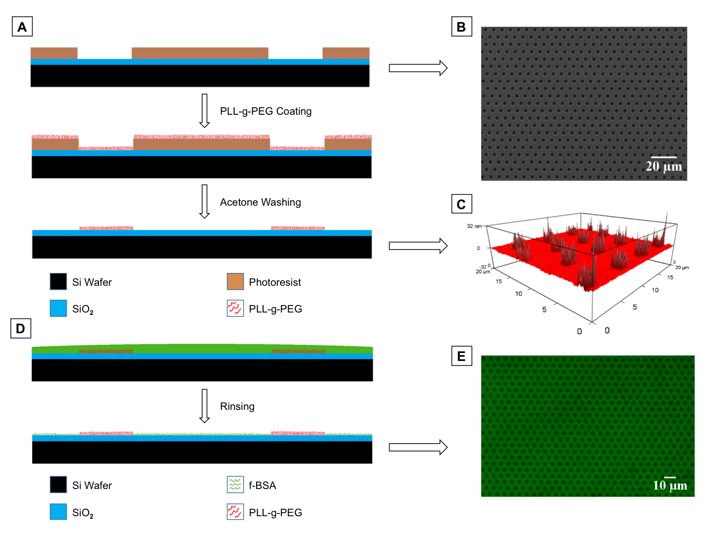
Figure 1. A. The prepration steps for PLL-g-PEG patterning, B. SEM image of surface after first step (photolithography), C. AFM height profile of the PLL-g-PEG-patterned substrate, D. Process design of patterning visualization using f-BSA, E.Visualization of final non-fouling micro-pattern using f-BSA.
Leave a Reply
You must be logged in to post a comment.