Excimer laser annealing of sputtered three-layer stack (1)
Hello everyone! I plan to write several posts in the next couple of weeks about the laser annealing of our sputtered three-layer stack. This laser annealing experiment is done at Center for Nanophase Materials Sciences (CNMS) at Oak Ridge National Laboratory (ORNL). It is a collaborational proposal we submitted at the end of last year and approved early this year. The CNMS offers the free use of their facilities which were written in the proposal. To begin with, I would like to welcome more comments on my posts since it’s not easy for me to attend our the GREATEST NRG meeting after I moved to Vanderbilt. I’ll start with some basic information about samples, laser, setup and so on.
Sample info: NSN stack with 50nm a-Si layer and 30nm Si3N4 protective layers and the Si substrate was removed

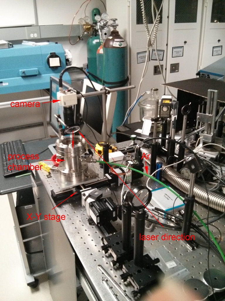
Laser info: pulsed KrF excimer laser, 248nm wavelength, 25ns FWHM, spot size: ~2.2 mm diameter

Experiment setup: Ar was flowing through the chamber during laser annealing.


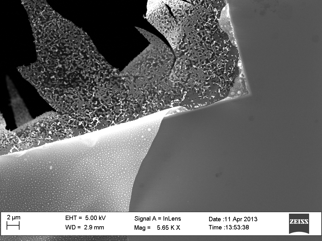
We have tried four different energy densities to do the laser annealing experiments. They are ~160mJ/cm2, ~110mJ/cm2, 80mJ/cm2 and 60mJ/cm2. The first set of images are samples annealed at around 160mJ/cm2. More than 50% of free-standing membranes broke during the laser annealing process at this energy density.
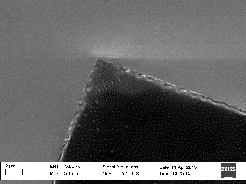

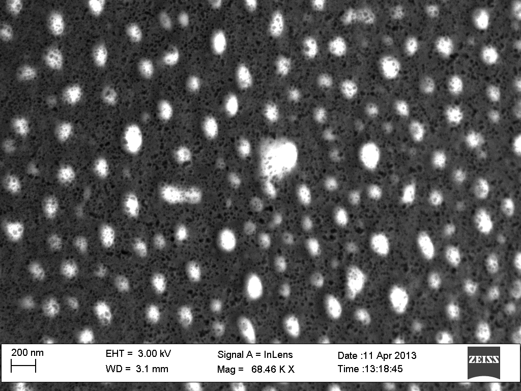
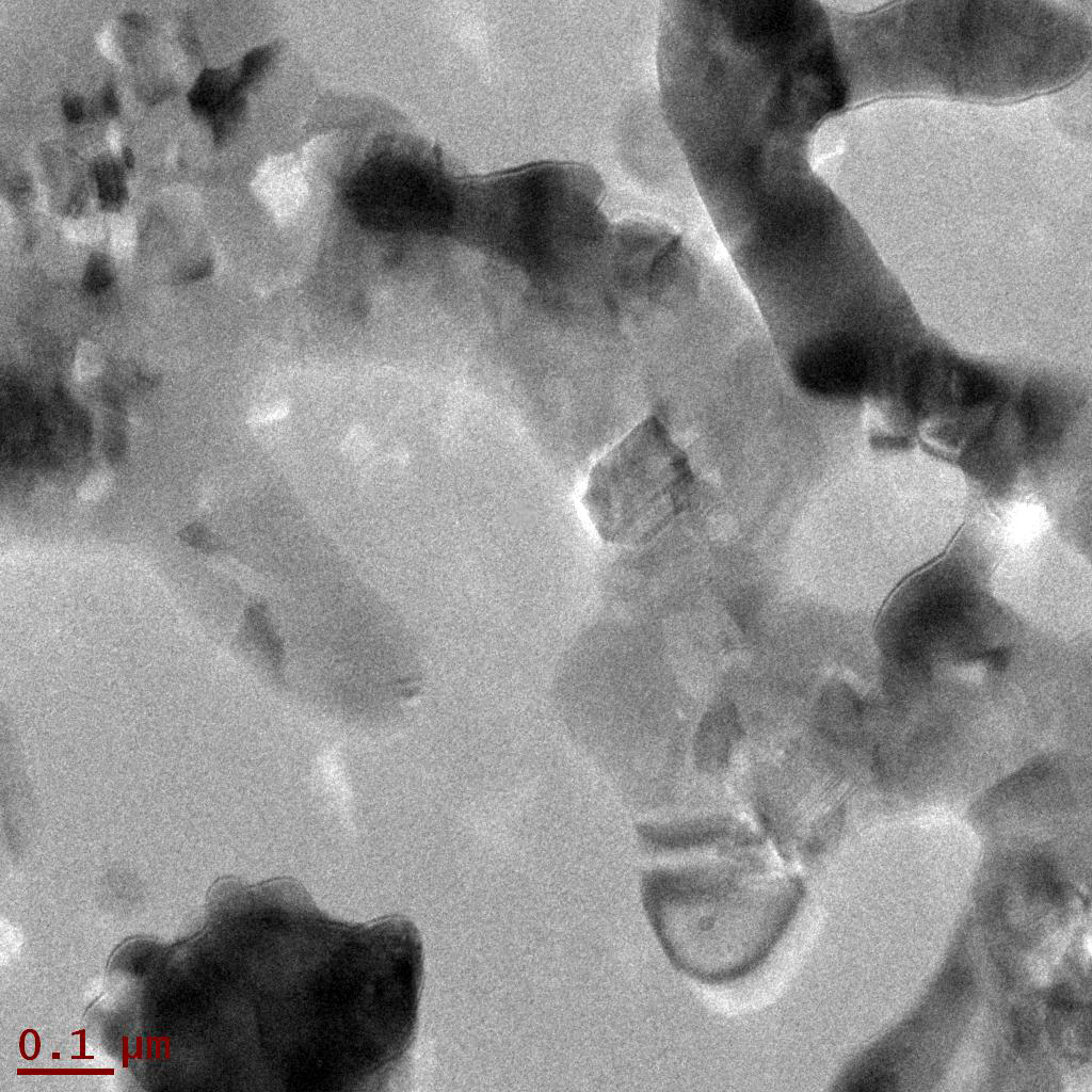
The top four are SEM images on the free-standing membrane area. First of all, it seems that the free-standing area shows a different morphology than the film on the substrate. This may due to the effect from the Si substrate as a sink to suck the heat from the top films through heat transfer where the free-standing stack absorbs all the energy from the laser. Second of all, the white dots feather looks like particles but it is not very clear at this point. Keep in mind that I didn’t strip nitride at this point and I believe they still sandwich the Si film. Another interesting feather would be the tiny dark dots feather, which looks like nanopores with 10 to 2onm in diameter. This also has not confirmed yet. A staff at CNMS helped me did a quick TEM on my samples and the followings are the TEM images of this sample.

From the TEM images, it first proves that those white area in the SEM image (black area in the TEM image) are not particles. The interesting part is that there are some feathers like void inside those black area in the TEM image. Another useful information from the diffraction image shows that Si film is partly crystallized. The majority part is still amorphous.
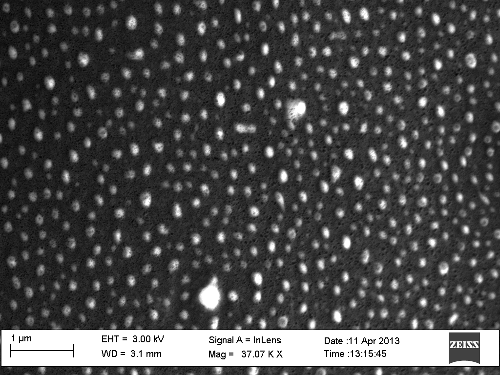
Next sample is annealed with energy density of 110mJ/cm2 and it shows very different results.


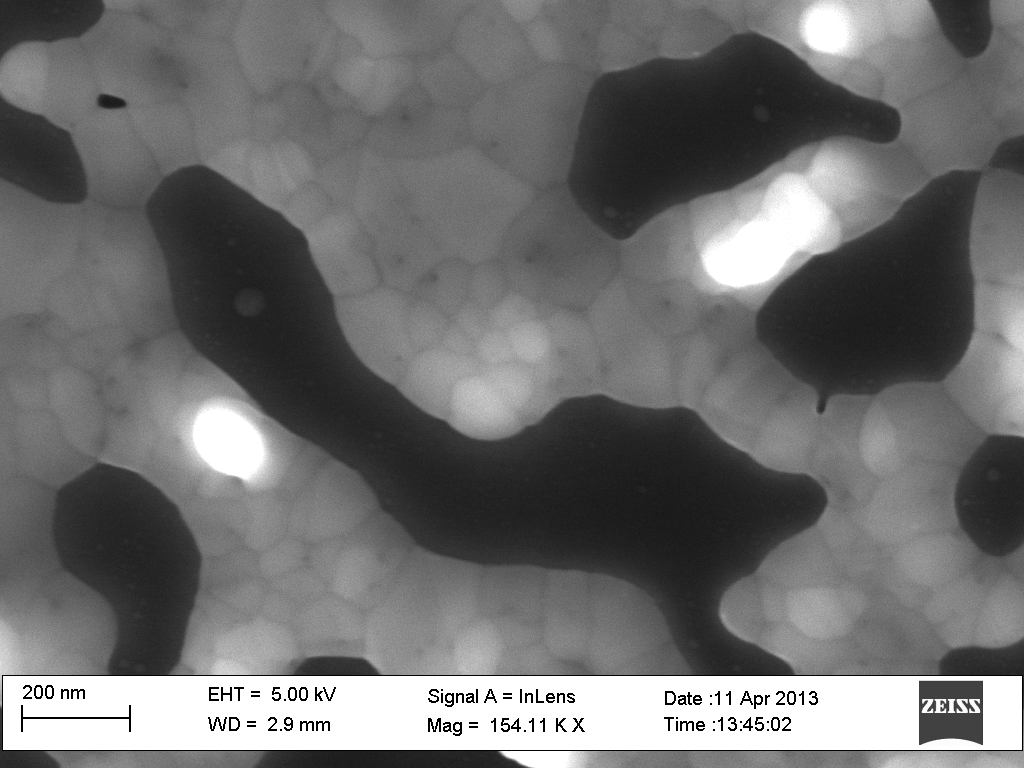
The top four SEM images are at different magnitude from low to high. This sample shows very different but interesting morphology that we have never seen in our RTP annealed samples. The SEM shows that Si film becomes to porous net structure after laser annealing! This porous net structure seems quite irregularly in terms of pores with different shapes and sizes. It also looks like unfinished Si agglomeration that Si film agglomerated to form tortured Si rods but still connecting to each other. Si grains and grain boundary can be clearly seen at a higher magnification. The size of Si grans ranges from several tens nanometers up to several hundreds nanometers. If you look at the images at lower magnitude carefully, you could see some quite bright spots. I believe these are bumped Si films (nodes ?) which have a higher height. Due to these bumped Si, the top nitride layer is pop out after annealing, which can be seen from some broken membranes at shown in the following.
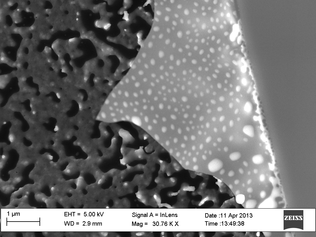
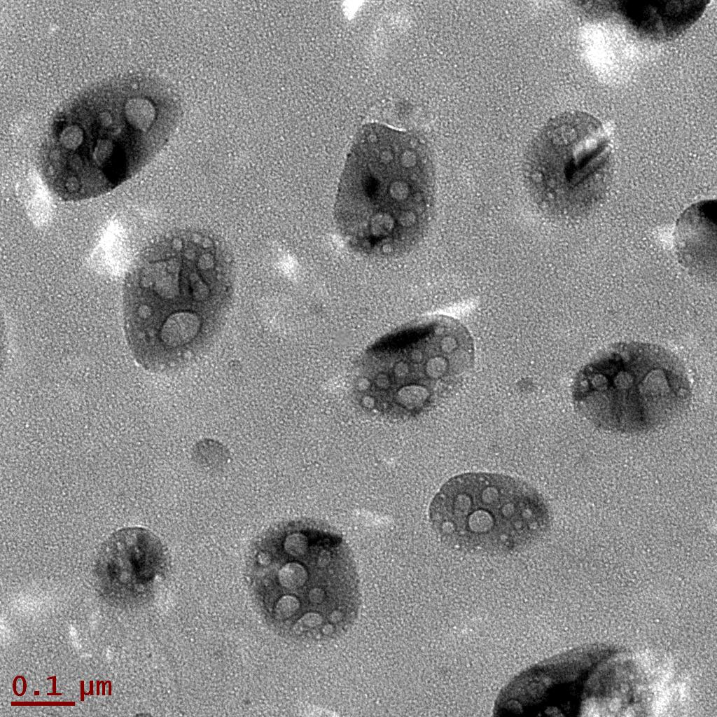
These are two interesting SEM images of the porous Si net structure with broken curved top nitride layer. The top nitride film shows some bright circular features which I think are some bumped features corresponding to the underneath bumped Si. In the second SEM image, the bended broken Si film shows a little cross-sectional view of the surface of the porous net structure Si, which seems pretty rough due to the bumped feature. Now let’s think this unique structure in a big picture, here is what happens in my thought. Si film tends to agglomerate during the laser annealing process at this energy density. However, the fully agglomeration is suppressed due to the existence of the cap/top nitride layer. Si film agglomerates to tortured porous net structure with different height in the thickness direction. These higher parts in the silicon film become to some bumpers with different sizes and the cap/top nitride layer deforms due to the compressive stress from these bumpers, which maybe the reason for the formation of the bulged structures. However, the compressive stress is quite big which can not offset by the plastic deformation of the silicon nitride and it results in the popping out the nitride film finally. This is a very preliminary speculation which needs to be further verified. The follows are some TEM images of this sample.
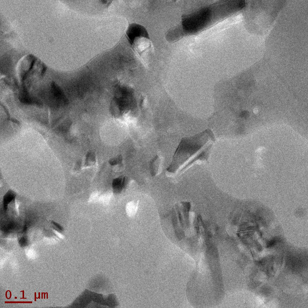

From the TEM images we can directly see the crystallized Si in tortured rod structure as well as the surrounded pores. The crystalline fraction seems pretty high in this sample.
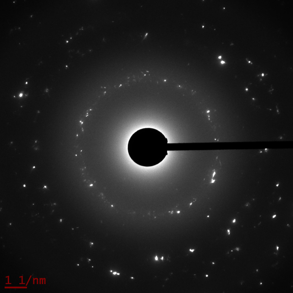
Samples which annealed at the rest two energy density seems not crystallize yet, which can be proved from the diffraction pattern of a sample annealed with 80mJ/cm2 in the following TEM images.

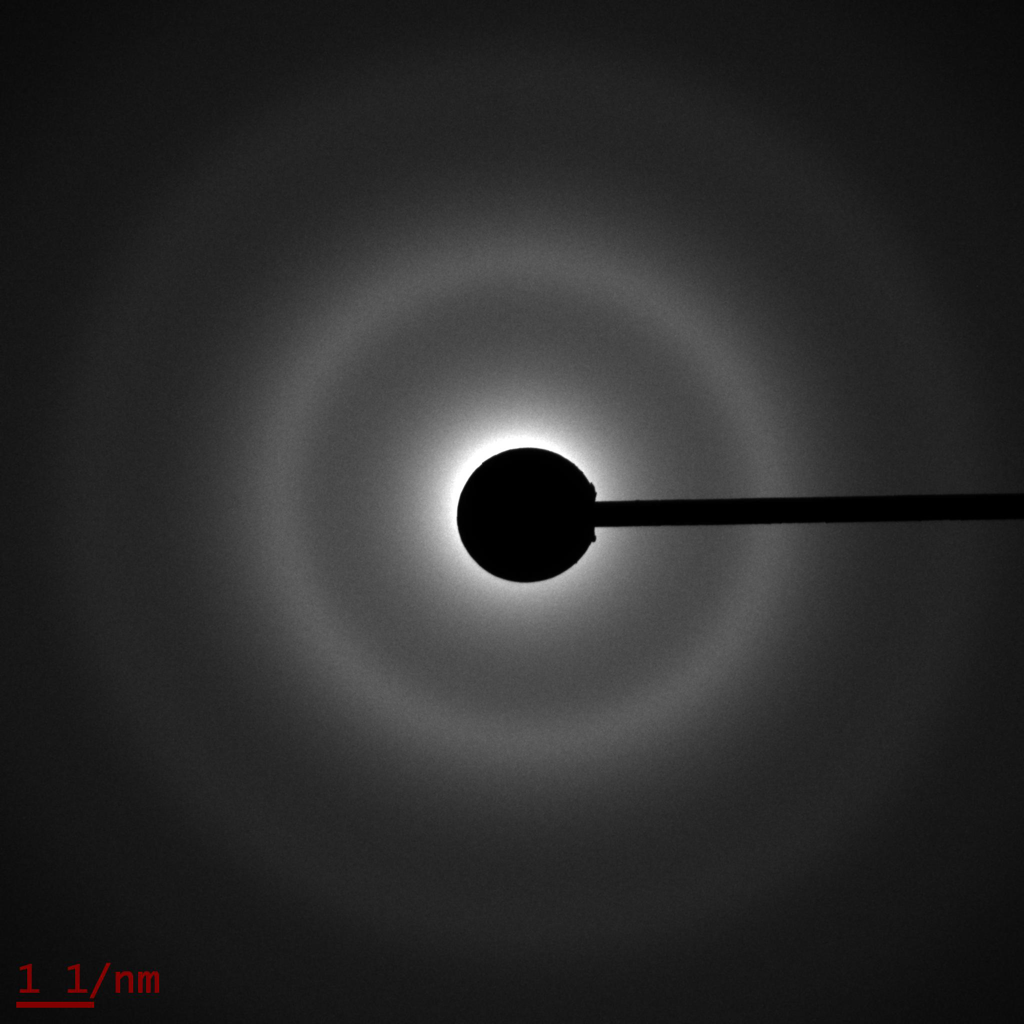
The bright view TEM image shows featureless amorphous phase and the diffraction pattern proves the amorphous nature of the silicon film. This means that the energy density of 80mJ/cm2 is not enough to crystallize amorphous silicon.
In sum, Si film shows very different morphologies with excimer laser annealing with different energy densities. Since this is our first attempt to crystallize Si film using excimer laser, further in-depth characterization of these interesting structures is needed to fully understand this different crystallization process. Any questions and comments are very welcome to bring in and would be very help for the further research.
It looks like you have melted/ablated the membrane. Why did you do this on free-standing material? The process should be much more controllable on films that are still on the wafer. For free-standing material, I think we have seen similar results with a little focused HeNe laser, when we have tried to do Raman. I think the advantage of this high power laser is that you could process material before you etch.
Thanks for sharing these results.
Hi Chris, thanks for the comments. The reason to do the annealing on single TEM grid is because it’s easy to do some TEM imaging right after the annealing and the spot size is around 2.2mm in diameter, which is big enough to cover the majority of the TEM grid. We can definitely do some laser annealing on the three-stack on Si wafer in the future. I don’t think the 110mJ/cm2 energy density is big enough to melt the Si film. From the reference the threshold fluence for surface melting is around 160mJ/cm2. Since this is our first experiment on excimer laser annealing and we don’t have any temperature measurement at this point. We are thinking about setting up another longer wavelength laser as a probe for the temperature measurement in the future.
Hey Joe, neat stuff!
I’m interested in understanding how much control you have over the laser. How do you modify the mJ/cm2? Is that just done by turning a power setting on the laser itself?
Can you change the spot size from 2.2mm by adjusting the focus of the beam on the sample?
Did these samples only see one 25 ns laser pulse? If so, could you try multiple pulses in rapid succession with the lower energy densities from you initial tests that did not have an effect?
Is there a reason not to try OSO instead of NSN? Do you expect any differences in absorption properties between the two materials?
I agree with Chris that looking at the membrane over the substrate would be more controllable. Why not do both? Just expect to use higher mJ/cm2 before you see results over the substrate.
Good luck!
Hey Josh, thanks for the questions. We added some glass plates between the laser and our sample to decrease the energy density that going to our samples. This is the way we used to change the energy density. I’m not very clear on how to change the spot size but the staff who built the setup seems to use some optical lenses to change the spot size. I can ask him for some details. We did single laser shot, double shots and triple shots the first time and almost all membranes broke after triple shots. I haven’t got a chance to look at into those sample with multiple shots. I personally believe that multiple shots would not affect the final result if the energy from the single shot is not enough to crystallize the Si. It’s like you heat the Si film to 500C for multi times but it wont’ crystallize the amorphous Si because the energy is lower than the threshold. We also did annealing on OSO samples and I haven’t characterize them yet. I’ll post new update once I get result.