BBB Device V2 Design
The goal of the design is to design a system that can co-culture cells under varying flow conditions, measure TEER, and perform dynamic microscopy. Specifically, the endothelial tight junctions are the primary mechanism by which the BBB is regulated. It is thought that astrocytes and pericytes can influence this mechanism. With the completed system, we should be able to observe the interaction between these cell types both optically and electrically to better understand the properties of the BBB. In the future, it should be possible to flow pharmacological agents and observe the effect on the BBB through fluorescence microscopy and TEER measurements. I have been working on a 3D drawing of my current design for the BBB device:
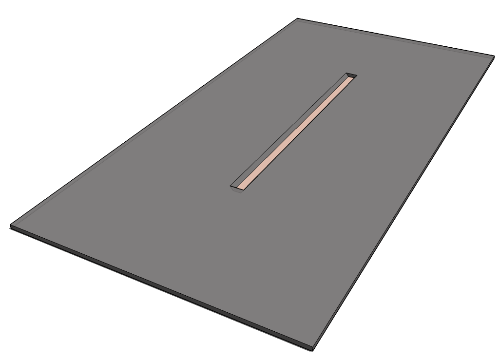
I’m looking to use a microporous membrane, to ensure that the astrocytic end-feet can invade the pores and contact endothelial cells on the other side of the membrane. The channel I have drawn here is 2cm long.
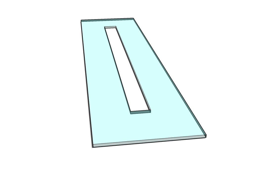
The gasket is an integral part to the design. Combined with the pnc-Si filter geometry, the gasket influences the overall shape of the channel that the cells reside in. This is important because the shape of the channel directly contributes to the flow profile that generates necessary shear stress on the endothelial cells. From this shear stress requirement, we can calculate the necessary pressure and volumetric flow needed to achieve this stress, summarized here
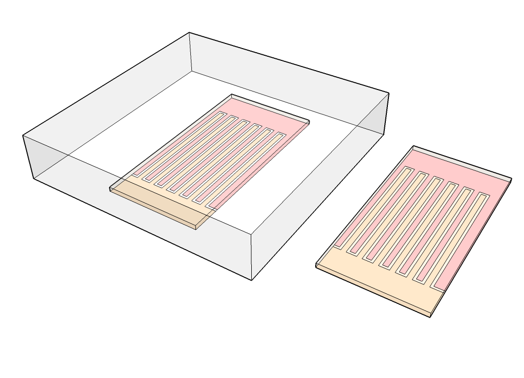
The advantage of the interdigitated design is that it samples the entire channel instead of relying a central point detection. Hopefully, this design will lead to consistent TEER recordings as the current is injected equally and sampled equally. It is easy to modify this design to create different voltage sampling points if necessary (TEER as a function of channel position), though ideally, the measurements should be very similar regardless of position. The electrode design can be used assuming an opaque metal for the electrode material. However, using a transparent conductive metal oxide, like indium tin oxide, obviates the need to leave large swaths of unmetalized open windows to see the cell growth in the channel. This particular design could probably optimized more; the design rules are generous. The blog post for creating these electrodes are found here and here

Lateral Crossection

Horizontal Crossection
The assembled component stack consists of the embedded electrode bonded to the silicone gasket (using mortar or corona wand bonding), which is then bonded to the filter using ozone bonding. I don’t know how the ITO film will respond to ozone bonding, but we can substitute mortar bonding at each step.

Some other ideas that I have been considering include making the gasket wider to provide better structural support and using a liner to modulate the channel depth height.